Page 20 - Chip Scale Review_March April_2022-digital
P. 20
FO-EB-T (where “T” represents through-  i n wh ich t he d ies a re ver t ically   layers of RDL with 2/2µm L/S, and
                                                                                                        2
        silicon via); in these structures, the top   interconnected. It is generally used to   the package size is 6,000mm , which
        dies are connected by a silicon bridge   connect the top low-power double data   is covered by a lid-type heat sink
        die and a RDL. The bridge die plays the   rate (LPDDR) memory with the bottom   on the top. Figure 2b shows that 6L
        main role with respect to communicating   system on chip (SoC) die. Therefore, the   RDLs are built up with C4 bumps for
        in the high-speed area between the die-  small form factor, thin package height   the  vertical  transmission  of  signal
        to-die structure. Because of the fine-  and low power consumption are the key   and power from active dies to the
        pitch and small L/S design, the metal   design factors for FO-PoP. Finally, FO-  substrate. The FO-MCM structure is
        L/S on the bridge die is normally smaller   MCM is another main platform that is   highly flexible for advanced package
        than 0.56µm. Therefore, compared to   widely applied in advanced packaging.   d e sig n i n t e r m s of t he C u w i r e
        2.5D, FO-EB only requires a small   In FO-MCM, the RDL connects the top   inside the RDL layers. FO-MCM is,
        silicon die size at the interconnect area,   dies horizontally using multi-layers of   therefore, also a robust platform for
        which reduces the interposer cost  by   RDL; and the L/S is generally scalable   both homogeneous and heterogeneous
        reducing the gross die size and raising   between 2/2µm~10/10µm. This flexible   integration, owing to the advantages of
        the yield performance for each interposer   routing design is better for power and   known-good RDL before die attaching
        wafer. Furthermore, FO-EB-T (which is   signal integrity. On the other hand, FO-  and a competitive manufacturing cost.
        designed using TSV structures) inside   MCM is the ideal structure to achieve a   Additionally, FO-MCM has a shorter
        the bridge die is the next cutting-edge   lower cost than 2.5D because the costly   development cycle time than 2.5D and
        packaging technology. Using a TSV   silicon interposer is not required [6-9].   FO-EB because the RDL interposer
        design in the FO-EB-T structure, the                                  can be grown before the wafer arrives
        electrical performance is enhanced by   Fan-out multi-chip module (FO-  at the outsourced assembly and test
        shortening the signal or power delivery   MCM) package technology     (OSAT) site for chip-last processing.
        path between the top die and the     The FO-MCM architecture is shown   T h e r ef o r e ,  FO - M C M  i s  w i d el y
        bottom substrate.                  in  Figure 2a. Three ASIC dies are   applied in chiplet integration because
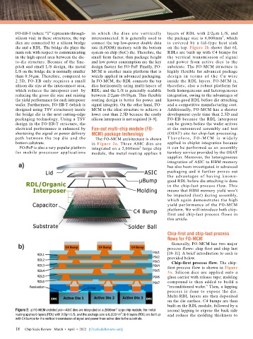
          FO-PoP is also a very popular platform   integrated on a 2,000mm  large chip   it  can be  performed as  an  assembly
                                                                  2
        for mobile processor applications   module, the metal routing applies 6   turnkey service provided by the OSAT
                                                                              supplier. Moreover, the heterogeneous
                                                                              integration of ASIC to HBM memory
                                                                              has also been investigated in advanced
                                                                              packaging and it further proves out
                                                                              the advantages of having known-
                                                                              good RDL before die attaching is done
                                                                              in the chip-last process f low. This
                                                                              means that HBM memory yield won’t
                                                                              be impacted (lost) during assembly,
                                                                              which again demonstrates the high
                                                                              yield  performance  of  the  FO-MCM
                                                                              platform. We will introduce both chip-
                                                                              first and chip-last process flows in
                                                                              this article.


                                                                              Chip-first and chip-last process
                                                                              flows for FO-MCM
                                                                                Generally, FO-MCM has two major
                                                                              process flows: chip first and chip last
                                                                              [10-11]. A brief introduction to each is
                                                                              provided below.
                                                                                Chip-first process flow. The chip-
                                                                              first process flow is shown in Figure
                                                                              3a. Silicon dies are applied onto a
                                                                              glass carrier with release tape; molding
                                                                              compound is then added to build a
                                                                              “reconditioned wafer.” Then, a lapping
                                                                              process is done to expose the die.
                                                                              Multi-RDL layers are then deposited
                                                                              on the die surface. C4 bumps are then
                                                                              built on the RDL module, followed by a
                                                       2
        Figure 2: a) FO-MCM architecture—ASIC dies are integrated on a 2000mm  large chip module, the metal   second lapping to expose the back side
        routing applies 6 layers (RDL) with 2/2µm L/S, and the package size is 6,000mm ; b) 6 layers (RDL) are built up   and reduce the molding thickness to
                                                         2
        with C4 bumps for the vertical transmission of signal and power from active dies to the substrate.
        18
        18   Chip Scale Review   March  •  April  •  2022   [ChipScaleReview.com]

