Page 43 - Chip Scale Review_May June_2021-digital
P. 43
of parts to be taken from a substrate;
        2) the production volume; and 3)
        production leveling. In particular,
        production leveling can avoid material
        wastes and reduce variable costs
        of production. For this production
        leveling, it is necessary to possess
        FOWLP technology complying with
        customers’ requests and to have a
        sufficient product portfolio.
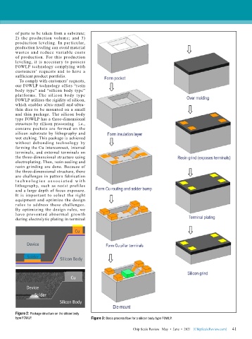
          To comply with customers’ requests,
        our FOWLP technology offers “resin
        body type” and “silicon body type”
        platfor ms. The silicon body type
        FOWLP utilizes the rigidity of silicon,
        which enables ultra-small and ultra-
        thin dies to be mounted on a small
        and  thin  package.  The  silicon  body
        type FOWLP has a three-dimensional
        structure by silicon processing—i.e.,
        concave pockets are formed on the
        silicon substrate by lithography and
        wet etching. This package is achieved
        without debonding technology by
        forming the Cu interconnect, internal
        terminals, and external terminals on
        the three-dimensional structure using
        electroplating. Then, resin sealing and
        resin grinding are done. Because of
        the three-dimensional structure, there
        are challenges in pattern fabrication
        tec h n o l o g i e s  a s s o c i a te d  w i t h
        lithography, such as resist profiles
        and a large depth of focus exposure.
        It is important to select the right
        equipment and optimize the design
        rules to address these challenges.
        By optimizing the design rules, we
        have prevented abnor mal grow th
        during electrolytic plating in terminal


        Figure 2: Package structure on the silicon body
        type FOWLP.                        Figure 3: Basic process flow for a silicon body type FOWLP.

                                                                                                             41
                                                               Chip Scale Review   May  •  June  •  2021   [ChipScaleReview.com]  41

