Page 38 - Chip Scale Review_May June_2021-digital
P. 38
have tighter fringes by the same ratio. Once   satisfy these constraints simultaneously by   have seen the support chip itself fracture
        the roll has been set, the entire fiber array can   using a single underlying support structure   before the bond between the fiber array and
        be lowered and the translational degrees of   for both the PIC and the fiber array as shown   the support chip fails. Moreover, having the
        freedom (x, y, z) can be optimized without    in Figure 3. This new method is made   epoxy applied far from the optical interface
        needing to further adjust the roll.  possible because the height of the PIC and   and the PIC also prevents any epoxy from
          As mentioned above, a challenge with   the height of the fiber cores within the fiber   entering the optical interface or from
        standard silicon-photonic packaging methods   array can be precisely matched to within   contaminating the surface of the chip.
        is that conventional epoxies like NEA123   a few microns, thereby leaving space for a   Further packaging of the bonded chip-
        (Norland Electronic Adhesive 123) yellow   thin adhesive bond line. The support chip   and-fiber-array module involves fixtures
        when exposed to blue light at moderate   can be made of the same substrate material   as shown in Figure 4a. After insertion and
        intensities, quickly degrading optical   as the PIC to reduce or eliminate differential   wire bonding into a ceramic pin-grid array
        coupling. To avoid this, the epoxy should be   thermal expansion/contraction. Additionally,   to make electrical connections to the ion-
        viscous and must not be applied directly in   the fiber array itself can also be made of   trap electrodes, the module is placed in a
        the optical interface—capillary forces lead to   silicon (instead of glass/quartz) to further   frame made from UHV-compatible plastic
        wicking of uncured adhesives into the joint   match thermal contraction between the   (PEEK) in order to manage and guide the
        if applied near the periphery, making this   photonics chip and fiber array.  fibers entering the fiber-array block. Space
        an untenable approach when working in the   First, the PIC is epoxied to the top of   is typically at a premium inside cryogenic
        visible spectrum.                  the support chip and then the fiber array is   systems, as well as inside small room-
          A further challenge in QIP applications   aligned to the PIC as described above. This   temperature UHV systems, so the fibers
        is the requirement to couple light into PICs   alignment is made significantly easier by   must be routed out of the plane of the PIC
        in UHV environments, in many cases   the fact that the roll and pitch degrees of   chip. Furthermore, this routing requires
        at cryogenic temperatures. While most   freedom are constrained by the underlying   strain relief to reduce stress on the fiber
        photonic technologies operate at room   support chip and the nearly matched heights   array and module. This strain-relief frame
        temperature, integrating photonics with   of the PIC and fiber array. Once the fiber   allows for more straightforward handling
        various other quantum technologies, such   array is placed down on the support chip it   of the packaged module and fiber ends, and
        as trapped ions and superconducting qubits   is naturally “level” with respect to the PIC   therefore, also simplifies connecting fibers
        (e.g., for remote entanglement generation or   because both are supported on the same   to the connectorized inputs of the fiber array
        for high-bandwidth classical control) will   surface (see Figure 4).  within the vacuum system.
        require photonic interconnects that survive   To affix the fiber array, cryogenic- or
        multiple thermal cycles to 4K and below   UHV-compatible epoxy is applied beneath   Performance
        while maintaining optical coupling. Even   the fiber array. This is a much larger surface   Ion trap PIC chips prepared in the
        room temperature atomic systems must be   area joint than just the optical interface of   manner described above have been operated
        baked to  several hundred degrees Celsius for   the PIC and fiber array and, therefore, can   in  UHV chambers, both at cryogenic
        many days before use, leading to a similar,   form a much stronger joint. In our tests we   temperatures for extended periods, and with
        but opposite, thermal robustness requirement.
          Conventional epoxies (e.g., NEA123)
        fracture during cool down to cryogenic
        temperatures because of stress. Commercially
        available epoxies designed for operation at
        cryogenic temperatures are generally not
        transparent over the entire visible range, and
        therefore, cannot be placed in the joint itself.
        These cryogenic epoxies (e.g., Masterbond’s
        EP21TCHT-1) also require long cures
        (18hrs at room temperature), and therefore,
        alignment must be maintained for this time
        period while curing. One approach is to
        initially tack the alignment of the photonics
        with the fiber array using a small amount of
        UV-curable epoxy and then reinforcing the
        joints with cryogenic-compatible epoxies.
        However, the underlying tack epoxy can fail
        during cool down if not completely reinforced
        by the cryogenic epoxy.
        Support via common substrate
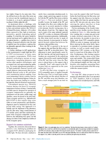
          Together, the constraints discussed above   Figure 3: Fiber array packaging via a common substrate. The top drawing shows a cross-section of a stack
        present a very challenging problem for   that allows for a common substrate to be mounted in a standard pin-grid-array package suitable for cryogenic
        cryogenic/UHV photonic packaging for   and UHV environments using standard-thickness Si-wafer spacers. The bottom drawing shows a plan view of
        visible light. We have devised a method to    the same structure when used with a square PIC chip (approximately 1cm on a side) and an offset fiber array on
                                           the support chip, which is serving as the common substrate (pin-grid-array not shown).

        36   Chip Scale Review   May  •  June  •  2021   [ChipScaleReview.com]
        36

