Page 39 - Chip Scale Review_May June_2021-digital
P. 39
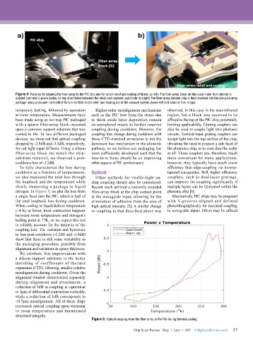
Figure 4: Fixtures for aligning the fiber array to the PIC chip and for strain relief and routing of fibers: a) (left) The fiber-array block (in this case made from silicon) is
        aligned and held in place during curing of adhesive between the block and common substrate; b) (right) The fiber-array bonded chip is then inserted into the pin-grid-array
        package using a vacuum-compatible fixture for fiber strain relief and routing out of the vacuum system (lower left and down in this image).
        temporary baking, followed by operation   Higher-order misalignment mechanisms   observed, in this case in the near-infrared
        at room temperature. Measurements have   such as the PIC bow from the stress due   region, but a block was required to be
        been made using an ion trap PIC packaged   to thick oxide layer deposition remain   affixed to the top of the PIC chip, potentially
        with a quartz fiber-array block mounted   an unexplored means to further improve   limiting applicability. Grating couplers can
        upon a common support substrate that was   coupling during cooldown. However, the   also be used to couple light into photonic
        cooled to 6K. In two different packaged   coupling loss change during cooldown with   circuits. Vertical-input grating couplers can
        devices, we observed that optical coupling   these CTE-matched structures is not the   accept light into the top surface of the chip,
        dropped by -2.8dB and -3.5dB, respectively,   dominant loss mechanism in the photonic   obviating the need to prepare a side facet of
        for red light input (674nm). Using a silicon   pathway, so we believe our packaging has   the photonics chip, or to even dice the wafer
        fiber-array block (to match the chip-  been sufficiently developed such that the   at all. These couplers are, therefore, much
        substrate material), we observed a post-  near-term focus should be on improving   more convenient for many applications,
        cooldown loss of -1.2dB.           other aspects of PIC performance.  however, they typically have much lower
          To fully characterize the loss during                               efficiency than edge-coupling via inverse-
        cooldown as a function of temperatures,   Outlook                     tapered waveguides. Still, higher efficiency
        we also measured the total loss through   Other methods for visible-light on-  couplers, such as dual-layer gratings,
        the loopback and the temperature while   chip coupling should also be considered.   can improve the coupling significantly if
        slowly immersing a package in liquid   Recent work utilized a convexly rounded   multiple layers can be fabricated within the
        nitrogen. In Figure 5, we plot the loss from   fiber-array block at the chip contact point   photonic chip [6].
        a single facet into the PIC, which is half of   at the waveguide input, allowing for the   Alternatively, PIC chips may be prepared
        the total loopback loss during cooldown.   elimination of adhesive from the area of   with V-grooves aligned and defined
        When cooling to liquid-helium temperature    high optical intensity [5]. A similar change   photolithographically for maximal coupling
        (~4 K) or lower, most contraction happens   in coupling to that described above was   to waveguide inputs. Fibers may be affixed
        between room temperature and nitrogen’s
        boiling point at 77K, so we expect this test
        to reliably account for the majority of the
        coupling loss. The variation and hysteresis
        in loss post-cooldown (-1.2dB and -1.8dB)
        show that there is still some variability in
        the packaging procedure, possibly from
        alignment and variations in epoxy thickness.
          We attribute this improvement with
        a silicon support substrate to the better
        matching of coefficients of thermal
        expansion (CTE), allowing smaller relative
        misalignment during cooldown. Given the
        alignment window characterized separately
        during alignment and attachment, a
        reduction of 3dB in coupling is equivalent
        to 1µm of differential contraction vertically,
        while a reduction of 1dB corresponds to
        <0.5µm misalignment. All of these chips
        recovered optical coupling upon warming
        to room temperature and maintained
        structural integrity.
                                           Figure 5: Optical coupling from the fiber array to the PIC during thermal cycling.

                                                                                                             37
                                                               Chip Scale Review   May  •  June  •  2021   [ChipScaleReview.com]  37

