Page 33 - Chip Scale Review_May June_2021-digital
P. 33
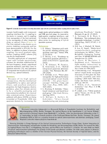
Figure 4: Schematic representation of an integrated atomic vapor cell with gradient-index surface coupling (GISC) to optical fibers.
        vacuum feedthroughs and evanescent   single-mode optical guidance to visible   pl a t fo r m  Pho t Pa c k ,” O p t i k
        coupling interfaces for: 1) coupling to   and NIR spectral range, by innovative   Photonik 10, pp. 42–47 (2015).
        the atoms in vacuum, and 2) coupling   light-matter coupling interfaces, and   7.  A. Ter vonen, B. R. West, S.
        from waveguides of the host substrate   by further development of hermetic   Honkanen, “Ion-exchanged glass
        to the waveguides of other integrated   glass joints for packaging of hybrid   waveguide technology: a review,”
        chips or optical fibers (Figure 4).   quantum systems.                     Optical Eng., 50(07), 071107, 1–15
        The first method is also known as an                                       (2011).
        atomic cladding waveguide and has   References                           8. S-H. Lee, J. Mitchell, W. Welch,
        been demonstrated in SiN [9]. For the   1.  E. Gibney, “Quantum gold rush:   S. Lee, K. Najafi, “Wafer-level
        latter, in addition to planar evanescent   the private funding pouring into   vacuu m / her metic packaging
        coupling, the novel gradient index      quantum start-ups,” Nature 574,    technologies for MEMs,” Proc.,
        surface coupling (GISC) scheme [10]     22-24 (2019).                      Reliability, Packaging, Testing,
        can also be implemented.             2. G. Moody, et al., “Roadmap on      and Char. of MEMS/MOEMS and
          Possible applications of integrated   integrated quantum photonics,”     Nanodevices IX, (2010).
        vapor cells include spectroscopy        arXiv:2102.03323v1 [quant-ph]    9.  L . S t e r n , B . D e s i a t o v, I .
        schemes for absolute stabilization of   (2021).                            Goykhman, et al., “Nanoscale
        the laser frequency, atomic vapor-based   3.  A. W. Elshaar i, W. Per nice,   light– mat ter  i nteractions  i n
        quantum memories and delay lines in     K. Srinivasan, et  al.,  “Hybrid   atomic cladding waveguides,”
        quantum networks [11], and realization   integrated quantum photonic       Nat. Comm. 4, 1548 (2013).
        of integrated non-reciprocal [12] optical   circuits,” Nat. Photonics 14, 285–  10.  J. Schwietering, et al., “Integrated
        devices (e.g., optical isolators).      298 (2020).                        optical single-mode waveguide
                                             4.  H. Schröder, et al., “Planar glass   structures in thin glass for flip-
        Summary                                 waveguides for high-performance    chip PIC assembly and f iber
          B e c a u s e o f i t s  h i g h o p t i c a l   electrical-optical circuit boards   coupling,” 2020 IEEE 70th Elec.
        transparency, ther mo-mechanical        ( E O C B) - t h e g l a s s - l a y e r-  Comp. and Tech. Conf. (ECTC),
        compatibility  to optics and  optical   concept,“ 53rd Elec. Comp. and     2020, pp. 148-155.
        f ib e r s , a nd exc el le nt d iele c t r ic   Tech. Conf., Proc., IEEE, 1053–  11.  C. Si mon, et  al.,  “Q u a nt u m
        properties for high-frequency electric   1059 (2003).                      memories,” Eur. Phys. J. D 58,
        guidance, glass has already proven   5.  L. Brusberg, H. Schröder, “Glass-  1–22 (2010).
        t o b e a valu able pa ck ag i ng a nd   based interposer and board-level   12. P. Lodahl, et al., “Chiral quantum
        interconnection platform for classical   packaging,” Chip Scale Review,    optics,” Nature, vol. 541, no. 7638,
        data communication. Experiences         July/Aug (2015).                   pp. 473–480. (2017).
        gathered with glassy EOCBs are being   6.  G .  B ö t t g e r,  S .  S e i f e r t ,  H .
        extended at Fraunhofer IZM into         S c h rö de r ,  “ G l a s s - b a se d
        quantum domain by increasing the        manufacturing and prototyping


                       Biographies
                         Wojciech Lewoczko-Adamczyk is a Research Fellow at Fraunhofer Institute for Reliability and
                       Microintegration (IZM), Berlin, Germany. He studied Physics at the Jagiellonian U. of Cracow, Poland,
                       and received a Doctoral degree from Humboldt U. in Berlin. After his post-doctoral fellowship at the U.
                       of Amsterdam, he held a research position at the Ferdinand-Braun-Institute, Berlin, Germany. He joined
                       Fraunhofer IZM in 2016 as a scientist focused on optical interconnections and photonic packaging. Email
                       Wojciech.Lewoczko-Adamczyk@izm.fraunhofer.de

            Henning Schröder is Group Manager of the Optical Interconnection Technologies Group (Dept. System Integration &
          Interconnection Technologies), at Fraunhofer Institute for Reliability and Microintegration (IZM), Berlin. He received his MSc
          in Applied Physics from the U. of Magdeburg, Germany, and his PhD at the Technical U. of Berlin. His main fields are R&D
          of optical interconnection technologies for printed circuit boards and photonic modules. He holds many patents in photonic
          packaging technologies and is a member of the German Physical Society, the German Society of Applied Optics, and the
          European Optical Society.


                                                                                                             31
                                                               Chip Scale Review   May  •  June  •  2021   [ChipScaleReview.com]  31

