Page 31 - Chip Scale Review_May June_2021-digital
P. 31
Glass-based quantum photonic packaging


        By Wojciech Lewoczko-Adamczyk, Henning Schröder  [Fraunhofer IZM]
        T        he ongoing second quantum


                 revolution is powered by
                 such quantum-mechanical
        phenomena as superposition, quantum
        ent a nglement, a nd i nter ference.
        Superposition suggests that a quantum
        particle, isolated from its environment,
        can exist at the same time in any
        combination of quantum states: different
        energy levels, spin, polarization, or
        even positions in space. Compared to
        the conventional bit, the basic building
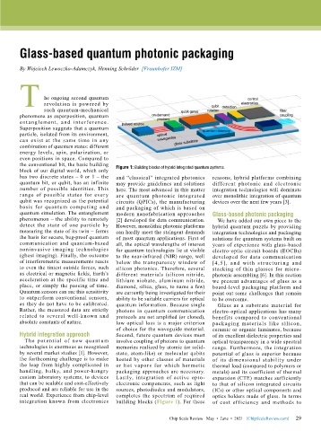
        block of our digital world, which only   Figure 1: Building blocks of hybrid integrated quantum systems.
        has two discrete states – 0 or 1 – the   and “classical” integrated photonics   reasons, hybrid platforms combining
        quantum bit, or qubit, has an infinite   may provide guidelines and solutions   different photonic and electronic
        number of possible identities. This   here. The most advanced in this matter   integration technologies will dominate
        range of possible states for every   are quant um photonic integrated   over monolithic integration of quantum
        qubit was recognized as the potential   circuits (QPICs), the manufacturing   devices over the next few years [3].
        basis for quantum computing and    and packaging of which is based on
        quantum simulation. The entanglement   modern nanofabrication approaches   Glass-based photonic packaging
        phenomenon – the ability to remotely   [2] developed for data communication.   We have added our own piece to the
        detect the state of one particle by   However, monolithic photonic platforms   hybrid quantum puzzle by providing
        measuring the state of its twin – forms   can hardly meet the stringent demands   integration technologies and packaging
        the basis for secure, bug-proof quantum   of most quantum applications. First of   solutions for quantum systems built on
        communication  and  quantum-based   all, the optical wavelengths of interest   years of experience with glass-based
        noninvasive imaging technologies   for quantum technologies lie at visible   electro-optic circuit boards (EOCBs)
        (ghost imaging). Finally, the outcome   to the near-infrared (NIR) range, well   developed  for  data  communication
        of interferometric measurements reacts   below the transparency window of   [4, 5], a nd w it h st r uc t u r i ng a nd
        to even the tiniest outside forces, such   silicon photonics. Therefore, several   stacking of thin glasses for micro-
        as electrical or magnetic fields, Earth’s   different materials (silicon nitride,   photonic assembling [6]. In this section
        acceleration at the specific time and   lithium niobate, aluminum nitride,   we present advantages of glass as a
        place, or simply the passing of time.   diamond, silica, glass, to name a few)   board-level packaging platform and
        Quantum sensors can use this sensitivity   are currently being investigated for their   point out some challenges that remain
        to outperform conventional sensors,   ability to be suitable carriers for optical   to be overcome.
        as they do not have to be calibrated.   quantum information. Because single   Glass as a substrate material for
        Rather, the measured data are strictly   photons in quantum communication   electro-optical applications has many
        related to several well-known and   protocols are not amplified (or cloned),   benefits compared to conventional
        absolute constants of nature.      low optical loss is a major criterion   packaging materials like silicon,
                                           of choice for the waveguide material.   ceramic or organic laminates, because
        Hybrid integration approach        Second, future quantum devices must   of its excellent dielectric properties and
          T he potential of new quant u m   involve coupling of photons to quantum   optical transparency in a wide spectral
        technologies is enormous as recognized   memories realized by atomic (or solid-  range. Furthermore, the integration
        by several market studies [1]. However,   state, atom-like) or molecular qubits   potential of glass is superior because
        the forthcoming challenge is to make   hosted by other classes of materials   of its dimensional stability under
        the leap from highly complicated in   or hot vapors for  which  hermetic   thermal load (compared to polymers or
        handling, bulky, and power-hungry   packaging approaches are necessary.   metals) and its coefficient of thermal
        custom laboratory systems, to devices   Lastly, integration of active opto-  expansion (CTE) matches sufficiently
        that can be scalable and cost-effectively   electronic components, such as light   to that of silicon integrated circuits
        produced and are reliable for use in the   sources, photodiodes and modulators,   (ICs) or other optical components and
        real world. Experience from chip-level   completes the spectrum of required   optics holders made of glass. In terms
        integration known from electronics   building blocks (Figure 1). For these   of cost  efficiency and methods  to


                                                                                                             29
                                                               Chip Scale Review   May  •  June  •  2021   [ChipScaleReview.com]  29

