Page 26 - Chip Scale Review_May June_2021-digital
P. 26
body provides excellent rigidity, even when
                                                                              cutouts are required to keep the body surface
                                                                              away from critical high-speed surface traces
                                                                              on the PCB. For both single-ended (SE) and
                                                                              differential (DIFF) I/O signals, maintaining
                                                                              a consistent mechanical and electrical path
                                                                              is critical to maximizing test yields. During
                                                                              2021, we expect to see SE signals in the
                                                                              >8GHz range, and DIFF signals moving very
                                                                              quickly from the current 56Gb/s standard to
                                                                              112Gb/s [3].
                                                                                Finally, there are important application
                                                                              and use-model cases that must be considered.
                                                                              Because SLT setups run system code, their
                                                                              implementation will fan out to a broader set
                                                                              of users across the engineering organization
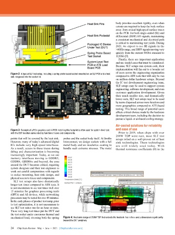
        Figure 2: A typical SLT test setup, including a spring-probe based socket mounted on an SLT PCB and a heat
        sink integrated into the socket lid.                                  compared to ATE tests that will only be run
                                                                              on million-dollar hardware setups. Beyond
                                                                              the IC test development engineering team,
                                                                              SLT setups may be used to support system
                                                                              engineering, software development, and even
                                                                              customer application development. Given
                                                                              their much smaller size, and dramatically
                                                                              lower costs, SLT test setups tend to be used
                                                                              by teams dispersed across more functions and
                                                                              more geographies compared to ATE-based
                                                                              testing. This broad range of potential users
                                                                              affects critical choices made by the hardware
                                                                              development team, including the decision to
                                                                              pursue a liquid- or air-based cooling strategy.
                                                                              Air-cooled solutions for reliability
                                                                              and ease of use
        Figure 3: Example of a PCIe graphics card. A PCB matching this footprint is often used for system-level test,
        with the DUT location surrounded by functional traces and components.   Prior to 2019, when chips with over
                                                                              200W TDP were rare, most SLT test
        points that will be covered by the heat sink.   probes and the socket body itself. At Smiths   setups relied on a well-proven set of heat
        However, many of today’s advanced digital   Interconnect, we design sockets with a full   sink technologies. These technologies
        ICs include very high-speed interfaces.   metal body and an insulative coating to   are still widely used today. With
        As a result, access to these traces during   handle such extreme stresses. The metal   thermal resistance coefficients (ϴ) in the
        debug and characterization is becoming
        increasingly important. Today, as we see
        memory interfaces moving to GDDR5,
        GDDR6, GDDR6x and beyond, the area
        around the DUT becomes critical, requiring
        system designers and their test engineers to
        work out careful compromises with regards
        to socket mounting, heat sink design, and
        physical access to traces and components.
          SLT test setups also have dramatically
        longer test times compared to ATE tests. It
        is not uncommon to see test times well over
        15 minutes for graphics processing units
        (GPUs) and AI devices, while networking
        processors may be tested for over 45 minutes.
        In the early phases of product test ramp, prior
        to test optimization, it is not uncommon to
        see SLT test suites run for an hour or more.
        These very long test times put the DUT and
        the test socket under enormous thermal and
        mechanical load, stressing both the spring   Figure 4: Heat sink design at 250W TDP that extends the heatsink fins in the x and y dimensions significantly
                                           beyond the DUT periphery.

        24   Chip Scale Review   May  •  June  •  2021   [ChipScaleReview.com]
        24

