Page 25 - Chip Scale Review_May June_2021-digital
P. 25
Cooling high-wattage digital ICs for socketed


        system-level test


        By Rick Marshall, Quynh Nguyen, Tim Wooden, Jiachun (Frank) Zhou  [Smiths Interconnect]
        M            odern  computing  and   are preferred because


                     networking applications
                                           mechanical durability.
                     are driving a new class   they deliver greater
        of digital integrated circuits (ICs) that have   SLT test environments
        enormous power dissipation requirements.   differ from ATE-based
        Built exclusively on the advanced 7nm and   setups in many critical
        5nm wafer fabrication nodes, these devices   ways. These differences
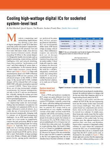
        have massive transistor counts, already   require an entirely   Table 1: Die size and transistor count trends for flagship GPUs from the
        exceeding 50 billion in the newest designs   n e w s e t of d e sig n   28nm process node to the state-of-the-art 7nm node.
        [1]. Designed to handle extreme tasks such as   considerations for a test
        graphics processing, crypto-mining, artificial   engineering group and
        intelligence (AI), and network switching,   its socket vendor. Critical
        these chips prioritize “performance at all   trade-offs must be made
        costs” such that reducing IC power draw is   to balance the electrical
        not a consideration. As the transistor density   test requirements against
        at these nodes increases, power density   the need for a reliable,
        follows suit (Table 1, Figure 1). Chips with   adequately cooled test
        sustained power draws over 300W of thermal   socket. Key among these
        design power (TDP) are now common, with   tradeoffs is deciding
        advanced designs in the 400W to 650W   whether to pursue an air-
        range. In the second half of 2021, multiple   cooled thermal solution,
        designs will be released that will average   or to make use of liquid
        800W TDP, with peak consumption expected   cooling.
        to exceed 1,000W. These large power
        draws are driving increasingly complex   System-level test   Figure 1: Increases in transistor density for GPUs from 2015 to present.
        requirements for thermal management,   hardware and use               ruled out based on mechanical considerations.
        not only in the IC’s end-use environment,   model                     Instead, the preferred option is to design a lid
        but, critically, during the testing activities   From a PCB and hardware standpoint,   for the test socket that integrates either air or
        required to debug, characterize, and produce   SLT setups are quite different from their   liquid cooling directly above the DUT.
        known-good-packaged parts.         ATE counterparts. ATE load boards are full-  To design a test socket and thermal
          In parallel with the trend noted above,   custom PCB designs, typically comprising   solution for SLT PCBs, the test engineering
        test engineering teams are increasingly   60+ layers, with trace routing and component   team and the socket vendor must overcome
        finding that deterministic test patterns run   placement designed specifically to enable   some unique challenges. Very often, the
        on automatic test equipment (ATE) are no   test. In contrast, SLT setups tend to use   system board has components and memory
        longer sufficient to catch all defects. As a   unmodified (or very slightly modified)   banks close to the processor that cannot
        result, the use of system-level test (SLT)   versions of the chip’s mission mode PCB,   be moved via a redesign. In simple cases,
        has increased dramatically, bringing with   complete with all the surrounding circuitry,   these keep-outs merely mean that the socket
        it a unique set of thermal management   memory banks, and external peripherals   thermal solution cannot extend beyond the
        challenges. As in ATE-based testing, SLT   present in the end use system. For compute or   x/y boundary of the socket body. In more
        setups use a test socket to temporarily   AI accelerator ICs, the PCB is likely to be a   complex cases, the adjacent memories will
        connect the ball grid array (BGA) or land   server motherboard of 8 to 16 layers that will   generate their own heat, and therefore,
        grid array (LGA) packaged part for testing   be slotted into a data center rack. For graphics   require either a separate or integrated cooling
        (Figure 2). Typically, these test sockets   or crypto-mining chips, the board is likely   solution. In cases where the components
        make use of a moving spring probe for   to be 6 to 8 layers in a peripheral component   around the DUT are of minimal height, an
        the electrical connection between the   interconnect express (PCIe) format (Figure 3)   oversize heat sink with an x/y footprint much
        printed circuit board (PCB) and the device   [2]. Because the layout of the area around the   larger than the DUT socket can be used, as
        ball or pad. Particularly at larger package   device under test (DUT) cannot be controlled   illustrated by the example in Figure 4. This
        sizes (over 40mm x 40mm), and at higher   by the SLT test engineering team, the use of   design approach assumes that the engineering
        power levels, spring probe interfaces   chamber-based thermal solutions is simply   team can live without probing access to the


                                                                                                             23
                                                               Chip Scale Review   May  •  June  •  2021   [ChipScaleReview.com]  23

