Page 21 - Chip Scale Review_May June_2021-digital
P. 21
The situations discussed above
        are just a  few  examples of how  die
 Advantest. Enabling the Age of    disaggregation and heterogeneous
        integration will stress the economics
 Convergence and Exascale Computing.  of test. One of the key challenges with
        heterogeneous integration will be
        how to architect manufacturing flows
        to manage yields. As the number of
        chiplets stitched together grows, the
        overall yield drops and the need for
        KGD grows. But delivering KGD out
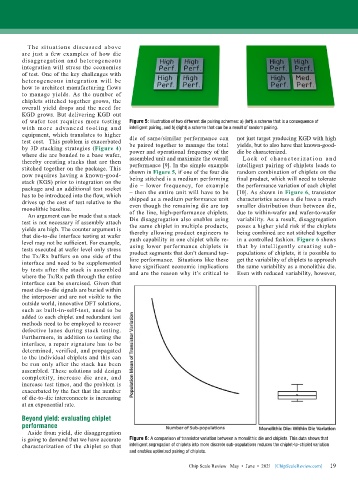
        of wafer test requires more testing   Figure 5: Illustration of two different die pairing schemes: a) (left) a scheme that is a consequence of
        with more advanced tooling and     intelligent pairing, and b) (right) a scheme that can be a result of random pairing.
        equipment, which translates to higher
        test cost.  This problem is exacerbated   die of same/similar performance can   not just target producing KGD with high
        by 3D stacking strategies (Figure 4)   be paired together to manage the total   yields, but to also have that known-good-
        where die are bonded to a base wafer,   power and operational frequency of the   die be characterized.
        thereby creating stacks that are then   assembled unit and maximize the overall   L a c k of c h a r a c t e r i z a t io n a n d
        stitched together on the package. This   performance [9]. In the simple example   intelligent pairing of chiplets leads to
        now requires having a known-good-  shown in Figure 5, if one of the four die   random combination of chiplets on the
        stack (KGS) prior to integration on the   being stitched is a medium performing   final product, which will need to tolerate
        package and an additional test socket   die – lower frequency, for example   the performance variation of each chiplet
        has to be introduced into the flow, which   – then the entire unit will have to be   [10]. As shown in Figure 6, transistor
        drives up the cost of test relative to the   shipped as a medium performance unit   characteristics across a die have a much
        monolithic baseline.               even though the remaining die are top   smaller distribution than between die,
          An argument can be made that a stack   of the line, high-performance chiplets.   due to within-wafer and wafer-to-wafer
        test is not necessary if assembly attach   Die disaggregation also enables using   variability. As a result, disaggregation
        yields are high. The counter argument is   the same chiplet in multiple products,   poses a higher yield risk if the chiplets
        that die-to-die interface testing at wafer   thereby allowing product engineers to   being combined are not stitched together
        level may not be sufficient. For example,   push capability in one chiplet while re-  in a controlled fashion. Figure 6 shows
        tests executed at wafer level only stress   using lower performance chiplets in   that by intelligently creating sub-
        the Tx/Rx buffers on one side of the   product segments that don’t demand top-  populations of chiplets, it is possible to
        interface and need to be supplemented   line performance.  Situations like these   get the variability of chiplets to approach
        by tests after the stack is assembled   have significant economic implications   the same variability as a monolithic die.
        where the Tx/Rx path through the entire   and are the reason why it’s critical to   Even with reduced variability, however,
        interface can be exercised. Given that
        most die-to-die signals are buried within
        the interposer and are not visible to the
        outside world, innovative DFT solutions,
        such as built-in-self-test, need to be
        added to each chiplet and redundant test
        methods need to be employed to recover
        defective lanes during stack testing.
        Furthermore, in addition to testing the
 A powerful synergy is taking place as high-performance computing intersects with     interface, a repair signature has to be
        determined, verified, and propagated
 artificial intelligence, causing a major shift in the evolution of semiconductor design. As   to the individual chiplets and this can
 the amount of data being processed grows exponentially and scalability creates new   be run only after the stack has been
 testing challenges, Advantest responds with the V93000 EXA Scale™ SoC Test Systems   assembled. These solutions add design
 offering solutions targeted at advanced digital ICs up to the exascale performance class.   complexity, increase die area, and
        increase test times, and the problem is
        exacerbated by the fact that the number
 As technologies continue to converge, Advantest is enabling its customers to address   of die-to-die interconnects is increasing
 Big Data and Smart Manufacturing challenges with innovative test solutions that ensure   at an exponential rate.
 superior performance of their most advanced device designs, and is helping them to   Beyond yield: evaluating chiplet
 quickly bring those products to market with the greatest cost efficiency.   performance
          Aside from yield, die disaggregation
        is going to demand that we have accurate   Figure 6: A comparison of transistor variation between a monolithic die and chiplets. This data shows that
        characterization of the chiplet so that   intelligent segregation of chiplets into more discrete sub-populations reduces the chiplet-to-chiplet variation
                                           and enables optimized pairing of chiplets.
 WWW .ADV ANTEST.COM
                                                                                                             19
                                                               Chip Scale Review   May  •  June  •  2021   [ChipScaleReview.com]  19

