Page 19 - Chip Scale Review_May June_2021-digital
P. 19
driving the need for loopback-based test
                                                                              methods in wafer test. These differences
                                                                              between wafer test and package test can
                                                                              result in higher yield loss downstream
                                                                              and the cost-benefit tradeoff of such
                                                                              approaches needs to be carefully
                                                                              considered when architecting the product
                                                                              and the manufacturing flow.
                                                                                A n o t h e r c o n s e q u e n c e o f  d i e
                                                                              disaggregation and heterogeneous
                                                                              integration is the need for a passive
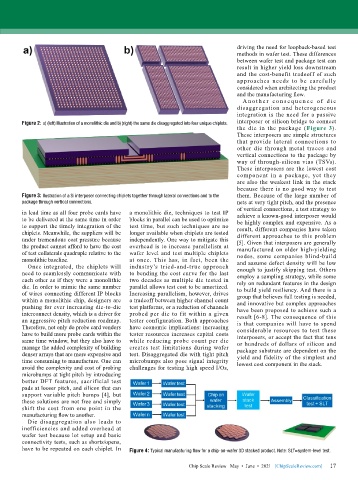
        Figure 2: a) (left) Illustration of a monolithic die and b) (right) the same die disaggregated into four unique chiplets.  interposer or silicon bridge to connect
                                                                              the die in the package (Figure 3).
                                                                              These interposers are simple structures
                                                                              that provide lateral connections to
                                                                              other die through metal traces and
                                                                              vertical connections to the package by
                                                                              way of through-silicon vias (TSVs).
                                                                              These interposers are the lowest cost
                                                                              component in a package, yet they
                                                                              are also the weakest link in the stack
                                                                              because there is no good way to test
        Figure 3: llustration of a Si interposer connecting chiplets together through lateral connections and to the   them. Because of the large number of
        package through vertical connections.                                 nets at very tight pitch, and the presence
                                                                              of vertical connections, a test strategy to
        in lead time as all four probe cards have   a monolithic die, techniques to test IP   achieve a known-good interposer would
        to be delivered at the same time in order   blocks in parallel can be used to optimize   be highly complex and expensive. As a
        to support the timely integration of the   test time, but such techniques are no   result, different companies have taken
        chiplets. Meanwhile, the suppliers will be   longer available when chiplets are tested   different approaches to this problem
        under tremendous cost pressure because   independently. One way to mitigate this   [5]. Given that interposers are generally
        the product cannot afford to have the cost   overhead is to increase parallelism at   manufactured on older high-yielding
        of test collaterals quadruple relative to the   wafer level and test multiple chiplets   nodes, some companies blind-build
        monolithic baseline.               at once. This has, in fact, been the   and assume defect density will be low
          Once integrated, the chiplets will   industry’s tried-and-true approach   enough to justify skipping test. Others
        need to seamlessly communicate with   to bending the cost curve for the last   employ a sampling strategy, while some
        each other as if they were a monolithic   two decades as multiple die tested in   rely on redundant features in the design
        die. In order to mimic the same number   parallel allows test cost to be amortized.   to build yield resiliency. And there is a
        of wires connecting different IP blocks   Increasing parallelism, however, drives   group that believes full testing is needed,
        within a monolithic chip, designers are   a tradeoff between higher channel count   and innovative but complex approaches
        pushing for ever increasing die-to-die   test platforms, or a reduction of channels   have been proposed to achieve such a
        interconnect density, which is a driver for   probed per die to fit within a given   result [6-8]. The consequence of this
        an aggressive pitch reduction roadmap.   tester configuration. Both approaches   is that companies will have to spend
        Therefore, not only do probe card vendors   have economic implications: increasing   considerable resources to test these
        have to build more probe cards within the   tester resources increases capital costs   interposers, or accept the fact that tens
        same time window, but they also have to   while reducing probe count per die   or hundreds of dollars of silicon and
        manage the added complexity of building   creates test limitations during wafer   package substrate are dependent on the
        denser arrays that are more expensive and   test. Disaggregated die with tight pitch   yield and fidelity of the simplest and
        time consuming to manufacture. One can   microbumps also pose signal integrity   lowest cost component in the stack.
        avoid the complexity and cost of probing   challenges for testing high speed I/Os,
        microbumps at tight pitch by introducing
        better DFT features, sacrificial test
        pads at looser pitch, and silicon that can
        support variable pitch bumps [4], but
        these solutions are not free and simply
        shift the cost from one point in the
        manufacturing flow to another.
          Die disaggregation also leads to
        inefficiencies and added overhead at
        wafer test because lot setup and basic
        connectivity tests, such as shorts/opens,
        have to be repeated on each chiplet. In   Figure 4: Typical manufacturing flow for a chip-on-wafer 3D stacked product. Note: SLT=system-level test.

                                                                                                             17
                                                               Chip Scale Review   May  •  June  •  2021   [ChipScaleReview.com]  17

