Page 18 - Chip Scale Review_May June_2021-digital
P. 18
Moore’s Law and the future of test


        By Pooya Tadayon, Greg Iovino, Sameer Ruiwale  [Intel Corporation]
        M            oore’s Law – wh ich   thought given that, at a per transistor   and the test industry. Addressing these


                     h a s  f u e l e d  t h e
                     semiconductor industry   level, it was several orders of magnitude   challenges in an economically viable
                                                                              manner is key to advancing Moore’s
                                           less  than  the  cost  to  manufacture  a
        for the last fifty years – is generally   transistor. As late as 1997, however, the   Law and will require a high degree of
        associated with the observation that   International Technology Roadmap for   innovation and collaboration from players
        the number of transistors on a chip   Semiconductors (ITRS) highlighted that   across the industry.
        doubles at a regular cadence. As   test cost per transistor was holding flat   Die disaggregation and heterogeneous
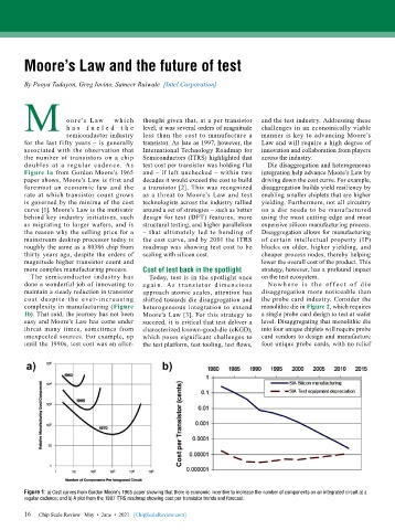
        Figure 1a from Gordon Moore’s 1965   and – if left unchecked – within two   integration help advance Moore’s Law by
        paper shows, Moore’s Law is first and   decades it would exceed the cost to build   driving down the cost curve. For example,
        foremost  an  economic law and the   a transistor [2]. This was recognized   disaggregation builds yield resiliency by
        rate at which transistor count grows   as a threat to Moore’s Law and test   enabling smaller chiplets that are higher
        is governed by the minima of the cost   technologists across the industry rallied   yielding. Furthermore, not all circuitry
        curve [1]. Moore’s Law is the motivator   around a set of strategies – such as better   on a die needs to be manufactured
        behind key industry initiatives, such   design for test (DFT) features, more   using the most cutting edge and most
        as migrating to larger wafers, and is   structural testing, and higher parallelism   expensive silicon manufacturing process.
        the reason why the selling price for a   – that ultimately led to bending of   Disaggregation allows for manufacturing
        mainstream desktop processor today is   the cost curve, and by 2001 the ITRS   of certain intellectual property (IP)
        roughly the same as a 80386 chip from   roadmap was showing test cost to be   blocks on older, higher yielding, and
        thirty years ago, despite the orders of   scaling with silicon cost.  cheaper process nodes, thereby helping
        magnitude higher transistor count and                                 lower the overall cost of the product. This
        more complex manufacturing process.  Cost of test back in the spotlight  strategy, however, has a profound impact
          The semiconductor industry has     Today, test is in the spotlight once   on the test ecosystem.
        done a wonderful job of innovating to   agai n. As t ra nsistor d i mensions   N o w h e r e i s t h e e f f e c t of d i e
        maintain a steady reduction in transistor   approach atomic scales, attention has   disaggregation more noticeable than
        cost  despite t he ever-i ncreasi ng   shifted towards die disaggregation and   the probe card industry. Consider the
        complexity in manufacturing (Figure   heterogeneous integration to extend   monolithic die in Figure 2, which requires
        1b). That said, the journey has not been   Moore’s Law [3]. For this strategy to   a single probe card design to test at wafer
        easy and Moore’s Law has come under   succeed, it is critical that test deliver a   level. Disaggregating that monolithic die
        threat many times, sometimes from   characterized known-good-die (cKGD),   into four unique chiplets will require probe
        unexpected sources. For example, up   which poses significant challenges to   card vendors to design and manufacture
        until the 1990s, test cost was an after-  the test platform, test tooling, test flows,   four unique probe cards, with no relief


        Figure 1: a) Cost curves from Gordon Moore’s 1965 paper showing that there is economic incentive to increase the number of components on an integrated circuit at a
        regular cadence; and b) A plot from the 1997 ITRS roadmap showing cost per transistor trends and forecast.

        16
        16   Chip Scale Review   May  •  June  •  2021   [ChipScaleReview.com]

