Page 13 - Chip Scale Review_May June_2021-digital
P. 13
technologies that require process-related
        development and changes, an adjustment
        in our new probe design does not
        slow down the process. With a simple
        software modification, the probe can be
        redesigned and manufactured within
        a very short period of time, with no
        changes to the process. In order to keep
        the costs and lead times of MEMS probe
        cards down, all, or as much as possible,
        of the manufacturing process is set up
        in-house.

        MEMS RF & high-power IC probing
          Nearly all semiconductor devices on
        the market today include an RF or higher
        speed component along with increased
        power domains that require entirely
        novel approaches to test. Considering
        that the characteristics of the physical
        probe are one of the main contributing
        factors to an efficient test solution, it
        is now more essential than ever to take
        a customizable pin approach when
        designing a probe card. The probe card
        must be capable of high frequency and
        higher power requirements, while at the   Figure 3: MEMS hybrid probe layout example.
        same time, have the capability to handle                              card design process and optimizing
        these stringent test conditions to prevent                            the stack-up is critical to allow for heat
        burning the probes. In addition, it must                              dissipation so the probes can pass higher
        meet electrical and increased parallelism                             current at elevated temperatures. In
        requirements, all of which lead to a                                  order to produce an ideal structure, we
        lower cost of probe card ownership.                                   start by experimenting with a variety
          Combining the test requirements                                     of materials. Then, by working with
        noted above, the need for higher                                      different configurations in the stack-up
        speed s, h ig her cu r rent- ca r r y i ng                            and performing finite element analysis
        capability and better signal integrity,                               (FEA) and electrical simulations,
        creates a challenge for a probe card                                  the optimal probe head design can
        solution that must accommodate all                                    be modif ied to the electrical and
        these  requirements  and  perform  to   Figure 4: MEMS hybrid probe head array.  mechanical requirements over a wide
        expectations. A proven MEMSFlex™                                      range of temperatures [1].
        solution for RF/high-power testing                                      Figure 6 illustrates two separate
        involves a hybrid probe head concept                                  probe head stack-ups, the guide plate
        manufactured with a combination of                                    gap variations, and the heat dissipation
        larger diameter probes for high-current                               comparison. During test, a tremendous
        and smaller diameter probes to handle                                 amount of current is going in and out
        the non-high-current portions of the IC                               of localized areas on the chip, typically
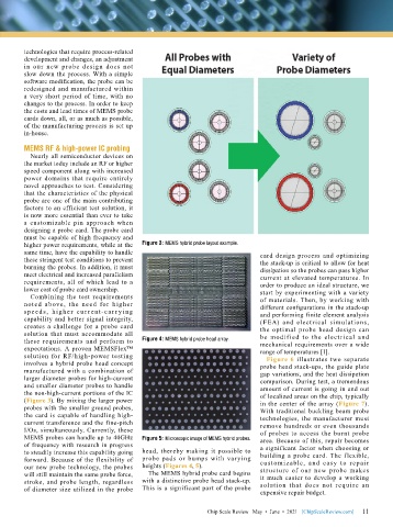
        (Figure 3). By mixing the larger power                                in the center of the array (Figure 7).
        probes with the smaller ground probes,                                With traditional buckling beam probe
        the card is capable of handling high-                                 technologies, the manufacturer must
        current transference and the fine-pitch                               remove hundreds or even thousands
        I/Os, simultaneously. Currently, these                                of probes to access the burnt probe
        MEMS probes can handle up to 40GHz   Figure 5: Microscopic image of MEMS hybrid probes.  area. Because of this, repair becomes
        of frequency with research in progress                                a significant factor when choosing or
        to steadily increase this capability going   head, thereby making it possible to   building a probe card. The flexible,
        forward. Because of the flexibility of   probe pads or bumps with varying    customizable, and easy to repair
        our new probe technology, the probes   heights (Figures 4, 5).        structure  of our  new  probe  makes
        will still maintain the same probe force,   The MEMS hybrid probe card begins   it much easier to develop a working
        stroke, and probe length, regardless   with a distinctive probe head stack-up.   solution that does not require an
        of diameter size utilized in the probe   This is a significant part of the probe   expensive repair budget.


                                                               Chip Scale Review   May  •  June  •  2021   [ChipScaleReview.com]  11 11

