Page 12 - Chip Scale Review_May June_2021-digital
P. 12
A new approach to testing ICs with MEMS


        By Raymond W. Grimm  [Nidec SV TCL]
        T        he expansion of 5G/Internet   Flexible and customizable MEMS


                 of Things (IoT) and the
                 i n c r e a s i ng  n u m b e r  o f   probe technology
                                             One of semiconductor’s leading
        semiconductors in automobiles, homes   technologies, microelectromechanical
        and other emerging technologies has   systems (MEMS), can be found in
        made it more important than ever that   nearly all new technology products from
        the equipment entrusted to test these   navigation, microphones, and medical
        integrated circuits (ICs) works effectively   devices to everything else in between. For
        and efficiently right out of the box. And   IC test, MEMS-based probe cards have
        if all of that was not enough, every new   become the breakout stars and are the
        chip design now includes some type of   fastest growing product segment. Because
        high-speed and high-power requirement   of the significant increase in the complexity
        for test. The speed and efficiency of test   of test, the number of probes required on a
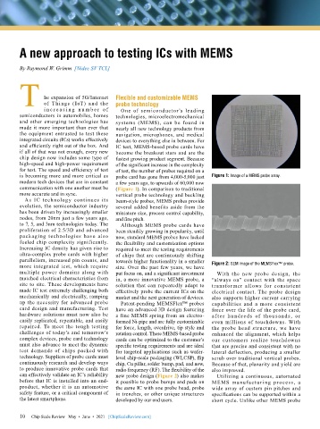
        is becoming more and more critical as   probe card has gone from 4,000-5,000 just   Figure 1: Image of a MEMS probe array.
        modern tech devices that are in constant   a few years ago, to upwards of 60,000 now
        communication with one another must be   (Figure 1). In comparison to traditional
        more accurate and in sync.         vertical probe technology and buckling
          As IC technology continues its   beam-style probes, MEMS probes provide
        evolution, the semiconductor industry   several added benefits aside from the
        has been driven by increasingly smaller   miniature size, process control capability,
        nodes, from 20nm just a few years ago,   and fine pitch.
        to 7, 5, and 3nm technologies today. The   Although MEMS probe cards have
        proliferation of 2.5/3D and advanced   been steadily growing in popularity, until
        packaging technologies have also   now, standard MEMS probes have lacked
        fueled chip complexity significantly.   the flexibility and customization options
        Increasing IC density has given rise to   required to meet the testing requirements
        ultra-complex probe cards with higher   of chips that are continuously shifting
        parallelism, increased pin counts, and   towards higher functionality in a smaller
        more integrated test, which require   size. Over the past few years, we have   Figure 2: SEM image of the MEMSFlex™ probe.
        multiple power domains along with   put focus on, and a significant investment   With the new probe design, the
        matched electrical characteristics from   in, a more innovative MEMS probe, a   “always on” contact with the space
        site to site. These developments have   solution that can repeatedly adapt to   transformer allows for consistent
        made IC test extremely challenging both   effectively probe the current ICs on the   electrical contact. The probe design
        mechanically and electrically, ramping   market and the next generation of devices.   also supports higher current carrying
        up the necessity for advanced probe   Patent-pending MEMSFlex™ probes   capabilities and a more consistent
        card design and manufacturing. Test   have an advanced 3D design featuring   force over the life of the probe card,
        hardware solutions must now also be   a fine MEMS spring from an electro-  af ter hu nd red s of t hou sa nd s, or
        easily replicated, repeatable, and easily   formed Ni-pipe and are fully customizable   even millions of touchdowns. With
        repaired. To meet the tough testing   for force, length, overdrive, tip style and   the probe head  structure, we  have
        challenges of today’s and tomorrow’s   rotation control. These MEMS-based probe   enhanced the alignment, which helps
        complex devices, probe card technology   cards can be optimized to the customer’s   our customers realize touchdowns
        must also advance to meet the dynamic   specific testing requirements and are ideal   that are precise and consistent with no
        test demands of chips packed with   for targeted applications such as wafer-  lateral deflection, producing a smaller
        technology. Suppliers of probe cards must   level chip-scale packaging (WLCSP), flip   scrub over traditional vertical probes.
        continuously research and develop ways   chip, Cu pillar, solder bump, pad, and now,   Because of that, planarity and yield are
        to produce innovative probe cards that   radio frequency (RF). The flexibility of the   also improved.
        can effectively validate an IC’s reliability   new probe design (Figure 2) also makes   Utilizing a continuous, automated
        before that IC is installed into an end-  it possible to probe bumps and pads on   MEMS manufact uring process, a
        product, whether it is an automotive   the same IC with one probe head, probe   wide array of custom pin pitches and
        safety feature, or a critical component of   in trenches, or other unique structures   specifications can be supported within a
        the latest smartphone.             developed by our end users.        short cycle. Unlike other MEMS probe


        10   Chip Scale Review   May  •  June  •  2021   [ChipScaleReview.com]
        10

