Page 32 - Chip Scale Review_May June_2021-digital
P. 32
By means of high-energy sputtering
                                                                              or thermal vapor deposition, glass
                                                                              can be covered with a broad range
                                                                              of metals. The metallization can
                                                                              be precisely str uctured with f ine
                                                                              lithographic techniques to provide
                                                                              high-quality guiding lines for direct
                                                                              current (DC), high-frequency (HF),
                                                                              and microwave signals up to 50GHz.
                                                                              In this manner, glass provides a high
                                                                              integration potential  by combining
                                                                              electrical and optical functionalities in
                                                                              one single EOCB substrate (Figure 3).
                                                                                Finally, compared to metals, glass
                                                                              has superior properties concerning a
                                                                              low outgassing rate and permeability
                                                                              for atmospheric gases, and therefore,
                                                                              has successf ully been used as a
                                                                              material for ultra-high vacuum (UHV)
                                                          2
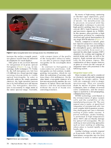
        Figure 2: Optical waveguides buried in ion-exchange process into a 400x300mm  panel.
                                                                              chambers for cooling and trapping of
        increase the surface strength, panel-  with a proper choice of the profile   neutral atoms and ions, as well as for
        size glasses benefit from the industrial   of the waveguide’s refractive index,   passive, high-vacuum spectroscopy
        developments for touch displays.   we  are able to  process single-mode   cells for hot atomic vapors. The
          Thin glass is an excellent material   waveguides for the wavelengths down   combination of these unique features
        for  integration  of  in-plane  optical   to 830nm.                   of glass is a basis for the concept of
        waveguides (Figure 2), e.g., by ion-  I n c o nt r a s t t o waveg u id e s o n   integrated vapor cells presented in the
        exchange (IoX) techniques [7]. Unlike   s e m i c o n d u c t or  pl at for m s ,  IoX-  following section.
        Si, the IoX-waveguides are low loss   waveguides are low-contrast, weakly-
        (<0.1dB/cm) in a broad spectral range   guiding waveguides, which do not   Integrated vapor cells
        covering telecom down to visible   allow for realization of curvature radii   Glass vacuum cells can be considered
        optical waveleng ths. In order to   lower than a few millimeters. On the   as a hermetic and optically transparent
        optically address the single quantum   other hand, a waveguide diameter of a   package for atomic qubits. Such
        emitters, the light intensity pattern   few microns perfectly matches the core   cells are commonly used in atomic
        has to be well defined on a sub-micron   diameter of optical fibers and thereby   s p e c t r o s c opy. T hey a r e u s u a l ly
        scale.  The  waveguides,  therefore,   ensures a low-loss interconnection   made by means of glass blowing
        have to necessarily be single mode in   w i t hou t t h e n e e d of b e a m - s i z e   techniques, have a volume of several
        the entire spectral range. Currently,   converting structures.        cubic centimeters, and the atomic
                                                                              vapor is excited by a free-propagating,
                                                                              collimated laser beam.
                                                                                MEMS technology contributed to
                                                                              the miniaturization of glass vacuum
                                                                              c el l s a nd t he s c a l a bi l it y of t he
                                                                              manufacturing process [8]. The next
                                                                              natural step is wafer- or panel-level
                                                                              integration of miniaturized cells into
                                                                              more complex hybrid quantum systems.
                                                                              One challenging task here is hermetic
                                                                              sealing of glass under vacuum. A
                                                                              proven technique, anodic  bonding,
                                                                              is performed at high temperatures
                                                                              above 300°C and can thereby damage
                                                                              the optical IoX-waveguides. We are
                                                                              working on more promising approaches
                                                                              such as laser welding or soldering,
                                                                              where  glass  is  heated  rapidly  and
                                                                              locally, only.
                                                                                Another challenge currently targeted
                                                                              at Fraunhofer IZM is the ability to
                                                                              bend planar waveguides into the third
                                                                              dimension in order to realize optical
        Figure 3: Electro-optic circuit board.

        30   Chip Scale Review   May  •  June  •  2021   [ChipScaleReview.com]
        30

