Page 47 - Chip Scale Review_May June_2021-digital
P. 47

T h e p ho t o l i t ho g r a p h i c r e s i s t
                                                                              prof ile deter mines the for mation
                                                                              o f s o l d e r  b u m p s ,  w h i c h  a r e
                                                                              accomplished using electroplating.
                                                                              The  increased  size  of  the  solder
                                                                              bump  is  located  where  the  resist
                                                                              thickness is thinner than the bump
                                                                              thickness. When the bump thickness
                                                                              exceeds the resist thick ness, the
                                                                              bu m p g r ow t h h a p p e n s l at e r a l ly
                                                                              and the supply of plating solution
                                                                              increases. Consequently, the rate
                                                                              of plat i ng g r ow t h i s i nc r e a s e d .
                                                                              O ne possible  cou nter measu re  is
                                                                              to increase the f ilm thickness by
                                                                              i mprov i ng t he st e p c ove r age of
                                                                              the resist. However, consider ing
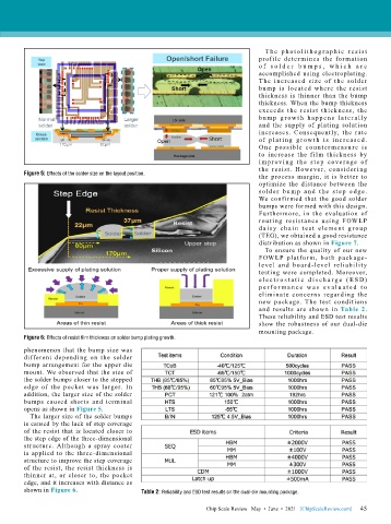
        Figure 5: Effects of the solder size on the layout position.          the process margin, it is better to
                                                                              optimize the distance between the
                                                                              solde r bu mp a nd t he  st e p  e dge.
                                                                              We confirmed that the good solder
                                                                              bumps were formed with this design.
                                                                              Furthermore, in the evaluation of
                                                                              routing resistance using FOW LP
                                                                              d a i s y ch a i n  t e s t ele m e nt  g r ou p
                                                                              (TEG), we obtained a good resistance
                                                                              distribution as shown in Figure 7.
                                                                                To ensure the quality of our new
                                                                              FOW LP platfor m, both package-
                                                                              level and board-level reliabilit y
                                                                              testing were completed. Moreover,
                                                                              e l e c t r os t a t i c  d isc h a r g e  ( E S D)
                                                                              p e r f o r m a n c e w a s e v a l u a t e d t o
                                                                              eliminate concer ns regarding the
                                                                              new package. The test conditions
                                                                              and  results  are  shown  in  Table  2.
                                                                              These reliability and ESD test results
                                                                              show the robustness of our dual-die
                                                                              mounting package.
        Figure 6: Effects of resist film thickness on solder bump plating growth.
        phenomenon that the bump size was
        different depending on the solder
        bump arrangement for the upper die
        mount. We observed that the size of
        the solder bumps closer to the stepped
        edge  of  the  pocket  was  larger.  In
        addition, the larger size of the solder
        bumps caused shorts and terminal
        opens as shown in Figure 5.
          The larger size of the solder bumps
        is caused by the lack of step coverage
        of the resist that is located closer to
        the step edge of the three-dimensional
        structure. Although a spray coater
        is  applied  to  the  three-dimensional
        structure to improve the step coverage
        of the resist, the resist thickness is
        thinner at, or closer to, the pocket
        edge, and it increases with distance as
        shown in Figure 6.                 Table 2: Reliability and ESD test results on the dual-die mounting package.

                                                                                                             45
                                                               Chip Scale Review   May  •  June  •  2021   [ChipScaleReview.com]  45
   42   43   44   45   46   47   48   49   50   51   52