Page 51 - Chip Scale Review_May June_2021-digital
P. 51
viscosity of the imprint materials induces   the forces resulting from the flow of the   working stamp 2 (Figure 1b). Dispensing
        resistance against the Z-axis movement.   viscous epoxy between the two stamps with   epoxy with precise volume and position is
        However, the active WEC technique can   arbitrary geometries. These forces can lead   extremely important in attaining the desired
        sustain a force up to 3kN, therefore, it plays   to a resulting shear force that generates a   final RLT while avoiding an overflow of
        a crucial role in accurately reaching the   shift in lateral directions. Furthermore, the   the epoxy. In the next steps, the fiducials
        targeted Z-position thereby spreading the   poor contrast of the fiducials on the PDMS   on stamp 2 are aligned to the grabbed
        epoxy to the desired thickness. Through   stamp (filled with epoxy) during the imprint   position of the fiducials on stamp 1. The
        its three-axis movement, it also allows for   process makes it challenging for the pattern   alignment with respect to grabbed positions
        a controlled re-leveling of the layers in the   recognition and automatic alignment   is needed because of the large gap of up
        machine if forces should induce changes in   systems. To mitigate this issue, back side   to 3mm between the two stamps, which
        the parallelism [4].               alignment (BSA; higher depth of focus)   makes it impossible to keep the targets of
          The use of silicone polymer stamps   is applied. BSA gives the opportunity to   both layers in focus at the same time. The
        on both sides of the imprint ensures   capture and train fiducials of the top stamp   combination of using the grabbed target
        the required high transfer fidelity. The   before the alignment features are concealed   position from stamp 1 and the live image
        combination of polydimethylsiloxane   by the epoxy, and allows for a direct view   from stamp 2 allows for reliable pattern
        (PDMS) and a rigid glass back plate   of the targets on the bottom stamp without   recognition and high accuracy alignment,
        provide, both the large area rigidity, and   interference of structures on the top stamp.  independent of the process gap between the
        the local flexibility, that is needed to   A general process flow of fabricating   two working stamps. In this paper, the RLT
        imprint monolithic arrays. The PDMS   monolithic lens arrays is represented   of the monolithic lens array is predefined
        part of the stamp assists the conformal   in Figures 1a-c. To begin with, the top   to be 200µm. Hence, the realignment and
        imprinting and thereby minimizes the   working stamp 1 is secured by vacuum on   Z-axis movement are performed until
        trapped air. Simultaneously, the rigid   the stamp holder and the bottom working   the target gap of 200µm is reached. After
        carrier provides the required in-plane   stamp 2 is held by vacuum on the bottom   reaching the targeted alignment and RLT,
        rigidity while imprinting to achieve   chuck. Once, the top and bottom stamps are   the epoxy is exposed for 6min by using the
        good TTVs. In order to achieve the very   fixed on their corresponding tooling, the   high intensity i-line band (365nm) from a
        good overlay accuracies needed for best   WEC process levels the two stamps with   broadband SUSS UV-LED unit (Figure 1c)
        optical performance, performing an X-Y   respect to each other. The alignment targets   [5]. In the final step, the cured free-standing
        alignment after each Z-axis movement step   on the working stamp 1 are captured using   monolithic lens array is separated from
        is obligatory until the final gap (and hence,   the BSA microscopes (Figure 1a). Then,   the working stamps, using a SUSS imprint
        the target RLT) is reached. This is due to   the epoxy is dispensed on the center of the   separation tool (Figure 1d).


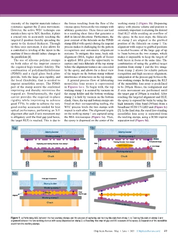
        Figure 1: a) Performing WEC between the two working stamps and the process of capturing and training fiducials from stamp 1; b) Training fiducials on stamp 2 and
        alignment between the two working stamps with epoxy dispensed on stamp 2; c) Reaching final imprint gap and UV-exposure of the epoxy; d) Separation of the monolithic
        stack from the working stamps.

                                                                                                             49
                                                               Chip Scale Review   May  •  June  •  2021   [ChipScaleReview.com]  49

