Page 53 - Chip Scale Review_May June_2021-digital
P. 53
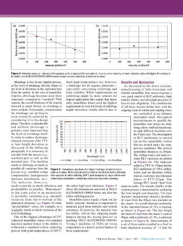
Figure 4: Refractive index vs. intensity of UV exposure: a) For a standard UV cure material, there is a clear tendency of lower refractive index with higher UV intensity to
        be visible; and b) DELO KATIOBOND OM614 shows a much reduced sensitivity to intensity variation.
          Shrinkage is key in any imprint process,   Such high temperatures are, however,   Results and discussion
        as the level of shrinkage directly relates to   a challenge for all organic materials—  As discussed in the above sections,
        the level of deviation of the replicated lens   especially concerning yellowing and   manufacturing of fully-functional and
        from the master. In the case of monolithic   form stability. While requirements on   reliable monolithic lens arrays requires a
        imprint, shrinkage becomes even more   yellowing might be more relaxed for   very good control of RLT uniformity, high
        important: compared to “standard” POG   imprint applications that require thin layers   transfer fidelity and ultra-high precision of
        imprint, the overall thickness of the imprint   only, monolithic lenses need the highest   lens-to-lens alignment. The combination
        material is much thicker, so shrinkage is   requirements as even low levels of yellowing   of all these factors define how well the
        more evident. Fortunately, compensation   might introduce visible effects due to   outgoing beam deviation and coupling losses
        for shrinkage can (at least to                                                are controlled in an ultimate
        some extent) be achieved by                                                   microoptics stack. All required
        considering it in the design                                                  measurements to qualify the
        phase. Therefore, a reproducible                                              monolithic lens arrays are done
        and uniform shrinkage is                                                      using a laser confocal microscope
        probably more important than                                                  at eight different locations over
        the level of shrinkage itself.                                                the 8-inch area. The investigation
        In order to reduce shrinkage-                                                 of RLT uniformity is carried
        induced variations (like TTV                                                  out on five monolithic wafers
        or lens height deviation as                                                   that are treated under the same
        discussed in the following                                                    process conditions. The desired
        paragraph), it is necessary to                                                monolithic thickness is 200µm.
        consider both the process (i.e.,                                              The within-wafer and wafer-to-
        machine) part as well as the                                                  wafer RLT variations are plotted
        material part. The machine                                                    in Figure 6a. The imprints
        needs to eliminate as much as                                                 achieve a TTV of <20µm and the
        possible all variations from the   Figure 5: Transmission spectrum of a 100µm-thick layer of optical imprint   RLT uniformity of <10%, within-
        process (e.g., excellent wedge  material on glass. While a typical polymer material would show severe yellowing   wafer, and are therefore within
        compensation, homogeneous  after exposure to reflow soldering (260°C peak temperature), major efforts were   typical customer specification
        intensity distribution, etc.).  undertaken to formulate a material that shows only very minor yellowing.  limits of TTV<25µm. The
        T he mater ial, however,                                                      average RLT varied <8µm from
        needs to provide as much robustness and   the rather high layer thickness. Figure 5   wafer-to-wafer. The transfer fidelity of the
        predictability as possible. “Robustness”   shows the transmission spectrum of DELO   imprint process is determined by evaluating
        in this sense refers to an insensitivity   KATIOBOND OM614 before and after the   the lens height and diameter. The lens
        to inevitable variations (e.g., intensity   reflow soldering process.  diameter measurements showed a deviation
        variation from top to bottom of the   Monolithic lenses require a hard, but not   of ±2µm from the 485µm lens diameter on
        imprinted structure, see Figure 4) while   brittle, material. Hardness is important to   the master. An overall diameter uniformity
        “predictability” refers, for example, to a   maintain good form stability and scratch   of the imprinted lenses of <1% is reached,
        negligible batch-to-batch variation of the   resistance. If, however, the material was   as shown in Figure 6b. The lens height
        level of shrinkage.                too brittle, effects like chipping might   deviation of ±3µm from the master’s value of
          One of the biggest advantages of UV-  happen during the dicing process or   90µm, with a uniformity of <3%, is achieved,
        replicated monolithic lenses over standard   handling. DELO KATIOBOND OM614’s   as shown in Figure 6c. Measurements of
        injection molded lenses is the ability to   Young’s modulus of 3GPa (at room   a set of three wafers resulted in a front to
        withstand a standard reflow soldering   temperature) is a near-to-perfect balance of   back alignment accuracy of  <1.3µm for
        process with peak temperatures of 260°C.   these requirements.

                                                                                                             51
                                                               Chip Scale Review   May  •  June  •  2021   [ChipScaleReview.com]  51

