Page 57 - Chip Scale Review_May June_2021-digital
P. 57
Evolution of thermal interface materials for


        advanced packaging


        By Andy C. Mackie, Ross Berntson  [Indium Corporation], Dave Saums  [DS&A LLC]
        H          igh-performance computing


                   (HPC) is becoming one
                   of the most impor tant
        factors driving growth in advanced
        semiconductor manufacturing. The
        pandemic of 2020-21 has driven widely-
        reported enormous increases in video
        data traffic, and with the growth and
        ubiquity of Internet of Things (IoT) in
        the form of 5G and self-driving cars and
        cloud-based artificial intelligence, HPC is
        here to stay.
          Although there is some debate over the
        shrinking logic node designator (7nm,
        5nm, 3nm, and so on) as a useful figure
        of die performance [1], and, indeed,
        whether it still has a physical relevance,
        it is interesting to note that the recent
        relatively modest improvements in
        transistor power consumption (currently
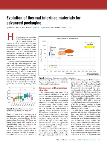
        only -20 to -30% per node shrink), are   Figure 2: Heat fluxes and temperatures for different applications.
        becoming overwhelmed by the increased   manufacturing defects [3]. Therefore,   decreased latency, the HBM must be
        density of transistors allowed by the   there is an increasing need to efficiently   placed close to the logic die. These HBM
        geometry reduction [2]. Average heat   cool these advanced node die.  die stacks are typically a different height
                                                                              when compared to the adjacent logic
                                           Heterogeneous and homogeneous      die, complicating the need for a one-
                                           integration                        stop thermal solution under a lid or heat
                                             While graphic processor units (GPUs)   sink (Figure 3). Further complicating
                                           are the current workhorses of the HPC   this situation is the increasing prevalence
                                           market, the long-term market trend is   of direct die-die bonding [5], such as
                                           towards application-specific ICs (ASICs)   Intel’s embedded multi-die interconnect
                                           [4]. Even though, through heterogeneous   bridge (EMIB), which adds to potential
                                           integration, memory and logic devices   complications in terms of non-coplanarity
                                           are increasingly found together under   of all die surfaces—another problem
                                           the heat spreader, the individual die area   that must also be addressed in the final
        Figure 1: Mean heat flux derived from product   for 7nm and smaller node devices is   reliable thermal solution.
        specification [2]. Courtesy of Dr. Yifeng Sun.  typically limited by extreme ultraviolet   In addition to memory stacks, which
                                           (EUV) reticle capabilities to 26 x 33mm.   may have individual die thicknesses of less
        fluxes per chip (that is, the amount of   Homogeneous integration, therefore,   than 20µm, logic die are also becoming
        heat generated per unit area of silicon)   consists of two or more identical logic   thinned to the point where substantial die
        are, therefore, growing (Figure 1). Die   die placed side-by-side on a substrate to   bowing may occur in the finished package.
                                     2
        backside heat fluxes over 150W/cm  are   increase the logic functionality. These   This is especially true for mobile HPC
        becoming common, with some areas of   smaller die also allow for significant   devices (often with logic die thicknesses
        very high heat flux (“hot spots”) on the   increases in die yield, as larger die are   of 150µm or less), where the z-axis
        die going much higher (Figure 2).  more susceptible to faults.        must be minimized to meet form factor
          It has been noted that as transistors   There is a need to thermally separate   criteria). However, there are also trends
        shrink, they become more sensitive to   the thin and thermally-sensitive high-  in non-mobile HPC towards die thinning,
        long-term exposure to high temperatures   bandwidth memory (HBM) stacks from   despite the absence of major form factor
        b e c au s e   of   i nc r e a s e d  n on -fa t a l   the logic. However, with the need for   constraints, as even the reasonably high


                                                                                                             55
                                                               Chip Scale Review   May  •  June  •  2021   [ChipScaleReview.com]  55

