Page 55 - Chip Scale Review_May June_2021-digital
P. 55
undergoing UV curing,  thereby providing   Ball Placement & Laser Soldering
        high dimensional stability. The epoxy
        also provided an excellent compatibility
        with the working stamp materials, thereby
        enabling a defect-free demolding of the
        cured monolithic lens array after the
        imprint process. In conclusion, we have
        demonstrated the capability of SUSS
        UV-imprint lithography and an optically
        tailored, UV-curable epoxy resin from
        DELO to manufacture freestanding,
        double-sided monolithic wafer-level
        optics. Therefore, wafer-level fabrication
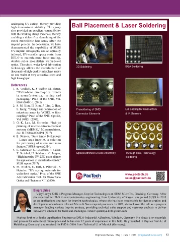
        technology allows the manufacture of       3D Soldering                    BGA Soldering
        thousands of high-quality microlens arrays
        on one wafer at very attractive costs and
        high throughput.

        References
          1. R. Voelkeli, K. J. Weible, M. Eisner,
            “Wafer-level microoptics: trends
            in manufacturing, testing and
            packaging,” Proc. of the SPIE, Vol.
            8169 81690C-1, (2011).
          2. S. M. Kim, H. Kim, J. Lim, J. Han,
            S. Kang, “Design and fabrication of   Presoldering of SMD              Lid Sealing for Connectors
            microlens array for VCSEL to fiber     Connector Elements             & IR Sensors
            coupling,” Proc. of the SPIE, Optifab,
            Vol. 10315,  (2005).
          3. G.-K. Lau, M. Shrestha, “Ink-jet
            printing of microelectromechanical
            systems (MEMS),” Micromachines,
            doi: 10.3390/mi8060194 (2017).
          4. E. Storace, “Suss Smile Technology
            – Large area imprint, a solution
            for patterning of micro and nano
            features,” SUSS report (2014).
          5. K. Schindler, U. Leischner, P. Kaiser,
            T. Striebel, U. Schömbs, C. lopper,    Optoelectronics Device Assembly  Through Hole Technology
            “High intensity UV-LED mask aligner                                    Soldering
            for applications in industrial research,”
            SUSS report (2017).
          6. M. Brehm, C. Ertl, I. Pilottek, P.
            Heissler, “UV curing materials for
            wafer-level optics,” Proc. of the SPIE                                www.pactech.de
            Adv. Fabrication Tech. for Micro/Nano                                 sales@pactech.de
            Optics and Photonics XIII (2020).


                       Biographies
                         VijayRamya Kolli is Program Manager, Imprint Technologies at, SUSS MicroTec, Garching, Germany. After
                       she received her PhD in microelectronics engineering from University of Kassel, she joined SUSS in 2015
                       as an applications engineer for imprint technologies, where she has been responsible for demonstration and
                       development of customer relevant Micro & Nano imprint processes. In 2021, she took over the role as a program
                       manager, leading various imprint projects, providing technical sales support and customer analysis to deliver
                       innovative solutions for technical challenges. Email vijaramya.kolli@suss.com

            Markus Brehm is Senior Application Engineer at DELO Industrial Adhesives, Windach, Germany. His focus is on materials
          and process for wafer-level microoptics and he has over 12 years of experience in this field. He graduated in Physics from U. of
          Heidelberg (Germany) and received his PhD in 2006 from Technical U. of Munich (Germany).


                                                                                                             53
                                                               Chip Scale Review   May  •  June  •  2021   [ChipScaleReview.com]  53

