Page 54 - Chip Scale Review_May June_2021-digital
P. 54
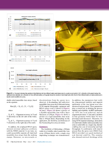
Figure 6: a) The graph indicates the variation in final thickness for four different wafers and shows overall, as well as each wafer’s, RLT uniformity; b) the graph displays the
        variation in lens diameter and uniformity for three different wafers; c) the graph shows the variation in lens height and uniformity for three different wafers; d) and e) pictures of a
        double-sided monolithic lens array.
        double-sided monolithic lens arrays, based    discolorations from the epoxy were   In addition, the parameters that verify
        on the equation:                   observed. A freestanding, full wafer-level   the dimensional stability and imprint
                                           monolithic lens array sheet fabricated using   uniformity of the lens layout were also
            Max [(X L  + X R  )/2 , (Y L  + Y R )/2)]  SUSS imprint lithography equipment and   discussed and presented. These parameters
                                           DELO epoxy resin is shown in Figures   play a crucial role in defining the process
          where                            6d and e. Figure 6d shows a picture of   stability and reliability. An RLT uniformity
                                           a flexible monolithic lens with a layer   of <10% has been achieved, and an
          X L  & Y L  : Alignment accuracy in X and   thickness of 200µm. Figure 6e shows a   alignment precision <1.3µm and a variation
        Y directions on the left side of the wafer;   picture of a rigid monolithic lens array   in lens geometry better than 3% were
        and                                that is 500µm thick. Depending on the   presented and discussed. Therefore, by
          X R  & Y R  : Alignment accuracy in X and   application, the flexibility and thickness of   using SUSS imprint technology, fabrication
        Y directions on the right side of the wafer.  the freestanding lens array are tuned.  of a full-wafer double-sided monolithic lens
                                                                              array is achievable in a single step, thereby
          In addition, the employed DELO epoxy   Summary                      enabling low cost of ownership and high
        showed minimal adhesion problems     The feasibility of fabricating a 200mm   throughput. In combination with imprint
        with the PDMS material. In our tests, we   wafer-level double-sided monolithic lens   process flow, the epoxy resin OM614 from
        could successfully separate all imprinted   array (200µm thick) with a single-step   DELO provided very good mechanical
        monolithic lens arrays from the working   imprinting technique was demonstrated.   and  thermal  stability. The  samples
        stamps. Moreover, no microcracks or                                   also showed minimal shrinkage while

        52
        52   Chip Scale Review   May  •  June  •  2021   [ChipScaleReview.com]

