Page 59 - Chip Scale Review_May June_2021-digital
P. 59
termed the system-level “thermal budget,”   The principal factors for determining
                                           with an increasing emphasis on the   a thermal budget are the maximum
                                           selection of appropriate TIM materials and   allowable die junction temperature
                                           their associated application processes. The   (generally T J ), the maximum allowable
                                           thermal budget comprises the heat transfer   case (semiconductor package external
                                           requirements and limitations (especially   surface) temperature (T C ); and the
                                           the highest allowable junction temperature   ambient temperature (T A ), as measured
                                           (T j MAX ) at the die transistor level) through   either internal to the system cabinet,
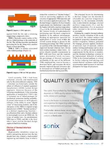
        Figure 5: Diagram of a TIM 0 application.  the various levels of semiconductor   or externally.
        against both the die and a retaining   packaging and thermal component   Defining the complete thermal pathway
        (supporting) compressive force.    hardware to the ambient environment.   involves careful evaluation of the needs
          TIM 1. Backside contact surface of the   Finding an appropriate material for   at each level, the contact surfaces and
        die in a lidded package to the underside of   application at every level within the   mechanical properties (chemical nature,
        the lid. The lid then provides mechanical   overall system design is driven by the   surface roughness, flatness, potential
        protection for the die, along with a modest   increasing percentage that TIMs represent   for warpage, pressure applied, thickness
        degree of heat spreading.          as a portion of the total thermal budget, as   of material, type of material, relative
          TIM 2. TIM 2 is always associated   improved thermal solutions have driven   surface wetting performance and so on) at
        with a lidded package (Figure 6).  total system resistance values lower.  As   each level, as well as the final reliability
                                           power density (usually synonymous in   requirements for the device or module,
                                           HPC with heat flux), and the requisite   and the thermal technology solution to
                                           power dissipation levels increase,   be implemented. Selection of suitable
                                           the percentage of thermal resistance   TIMs in the thermal pathway is critical
                                           attributable to the sum of the different   to further reducing total package and
                                           TIMs employed has risen to become a   system thermal resistance and to better
                                           dominant factor, and increases the drive   accommodate rapid increases in total heat
                                           towards improved thermal resistance due   dissipation for large die processors
                                           to increased use of lidded packages for
                                           mechanical protection during assembly.
        Figure 6: Diagram of TIM1 and TIM2 applications.
          Until recently, TIM 1 had been
        evaluated, selected, and implemented
        only by the semiconductor company. TIM
        1 selection was historically outside the
        sphere of influence of original equipment
        manufacturer  (OEM)  system  design
        engineers. However, because of the
        following considerations: 1) the increasing
        application of module-level TIM 0, due
        to increased use of lidded packages for
        mechanical protection during assembly;
        2) recent innovations in multi-physics
        software; 3) the ability to create “digital
        twins” of functioning modules; and 4) the
        emergence of the OEM or original design
        manufacturer (ODM) “thermal architect”
        as a distinct engineering function—
        specification of the entire thermal solution
        is increasingly seen as an OEM role. In
        terms of market size, the predominant
        TIM type is TIM2, and this is the level
        where most system thermal design
        engineers had been working.

        Choices of thermal interface
        materials
          High-profile reliability issues in
        mobile and gaming devices over the last
        decade have also created a much-needed
        engineering and industry focus in what is

                                                                                                             57
                                                               Chip Scale Review   May  •  June  •  2021   [ChipScaleReview.com]  57

