Page 48 - Chip Scale Review_May June_2021-digital
P. 48

Summary
                                                                               Our RISPAC technology addresses
                                                                             a w ide ra nge of dev ices for low-
                                                                             density applications. Silicon body
                                                                             ty pe FOWLP, which is one of our
                                                                             FOWLP technologies, is suitable for
                                                                             small and thin products with ultra-
                                                                             small and ultra-thin dies. The single-
                                                                             die  mounting  tech nology  we  call,
                                                                             silicon body type, is used for ultra-
                                                                             thin packages where the thickness can
                                                                             be up to 160μm maximum.
                                                                               Our dual-die mounting technology
                                                                             enables two dies to be mounted in a
                                                                             stack and electrically connected in
                                                                             a small, compact package, without
                                                                             h a v i ng t o u s e ex p e n s i v e T S V
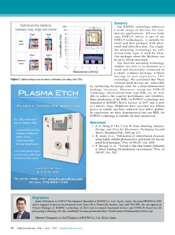
        Figure 7: Optimized layout and resistance distribution (of a daisy chain TEG).  technology. We confirmed that 90μm
                                                                             terminal pitch devices are  achievable
                                                             by optimizing the design rules for a three-dimensional
                                                             pa ck age st r uct u re. More ove r, u si ng ou r FOW LP
                                                             technology, called silicon body type RDL-1st, we were
                                                             able to achieve the required performance and reliability.
                                                             Mass production of the RDL-1st FOWLP technology was
                                                             launched at ROHM’s Kyoto factory in 2017 and is now
                                                             at a mature stage. Shipments have exceeded one billion
                                                             pieces in volume and have achieved zero-defect quality.
                                                             In conclusion, we have demonstrated that our RDL-1st
                                                             FOWLP technology is suitable for mass production.

                                                             References
                                                               1.  S. H. Zhang, F. Che, T. Lin, W. Zhao, Modeling, Analysis,
                                                                 Design, and Tests for Electronics Packaging beyond
                                                                 Moore, Woodhead Pub., 2019, pp. 2-3.
                                                               2.  H. Araki, et al., “Fabrication of redistribution structure
                                                                 using highly reliable photosensitive polyimide for fan-out
                                                                 panel-level packages,” Proc. of IWLPC, Oct. 2018.
                                                               3.  P. Metzger, et al., “Toward a flip-chip bonder dedicated
                                                                 to direct bonding for production environment,” Proc. of
                                                                 IWLPC, Oct. 2017.


                       Biographies
                         Isamu Nishimura is FOWLP Development Specialist at ROHM Co., Ltd., Kyoto, Japan. He joined ROHM in 1985
                       and is engaged in process development from 3μm LSI to 90nm LSI, memory lines and WLCSPs. He was appointed
                       Project Manager of RISPAC technology in 2014 and developed functional devices and FOWLPs based on LSI
                       processing technology. He also established its mass production lines. Email Isamu.Nishimura@lsi.rohm.co.jp

                         Mamoru Yamagami is a Staff Engineer at ROHM Co., Ltd., Kyoto, Japan.


        46   Chip Scale Review   May  •  June  •  2021   [ChipScaleReview.com]
        46
   43   44   45   46   47   48   49   50   51   52   53