Page 45 - Chip Scale Review_May June_2021-digital
P. 45
subst r at e side. T he se pro ce sse s
                                                                              a r e  f ol l owe d  b y  p e r f o r m a n c e
                                                                              testing, package saw, and tape and
                                                                              r e el, t o c omplet e t he a s se mbly.

                                                                              Single-die mounting technology
                                                                                T h e  a d v a n t a g e  o f s i n g l e - d i e
                                                                              mounting technology is that it makes
                                                                              ult ra-thin  packages  up  to  160μm
                                                                              maximum thickness possible. The
                                                                              mounting die’s size is available up
                                                                              to 0.2×0.2mm  minimum, and the
                                                                                            2
                                                                              t h ick ne ss  is  up  t o  80 μ m-10 0 μ m
                                                                              minimu m. T his package reduces
                                                                              damage to the mounting die because
                                                                              the thermal expansion coefficients
                                                                              of the mounting dies and the silicon
                                                                              substrate are the same, or nearly so.
                                                                              The rigidity of the package body also
                                                                              contributes to the reduction of damage
                                                                              to  the  mounting  dies.  In  the  front-
                                                                              end process before die mounting, the
                                                                              pocket etching to the silicon substrate
                                                                              and  the  photolithog raphy  on  the
                                                                              three-dimensional structure are key
                                                                              technologies to achieve this package.
                                                                                The pocket etching is performed
                                                                              using wet etching with a chemical
                                                                              solution. Because the sidewalls of the
                                                                              pockets are sloped by wet etching,
                                                                              we need to control the pocket depth
                                                                              va r iabi l it y i n orde r t o have t he
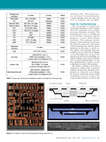
        Table 1: Package-level and board-level reliability test results on the single-die mounting package.  required space/distance between the


        Figure 4: An example of a dual-die mounting package and the package structure.

                                                                                                             43
                                                               Chip Scale Review   May  •  June  •  2021   [ChipScaleReview.com]  43

