Page 58 - ChipScale_Mar-Apr_2021-digital
P. 58
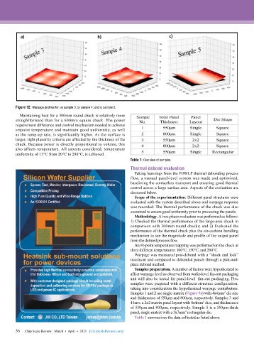
Figure 12: Warpage profiles for: a) sample 3; b) sample 4; and c) sample 5.
          Maintaining heat for a 300mm round chuck is relatively more
        straightforward than for a 600mm square chuck. The power
        requirement difference and control mechanism needed to achieve
        setpoint temperature and maintain good uniformity, as well
        as the ramp-up rate, is significantly higher. As the surface is
        larger, tight planarity criteria are affected by the thickness of the
        chuck. Because power is directly proportional to volume, this
        also affects temperature. All aspects considered, temperature
        uniformity of ±3°C from 20°C to 200°C, is achieved.
                                                             Table 1: Overview of samples.
                                                             Thermal debond evaluation
                                                               Taking learnings from the FOWLP thermal debonding process
                                                             flow, a manual panel-level system was made and optimized,
                                                             baselining the contactless transport and ensuring good thermal
                                                             control across a large surface area. Aspects of the evaluation are
                                                             discussed below.
                                                               Scope of the experimentation. Different panel structures were
                                                             evaluated with the system described above and warpage response
                                                             was recorded. The thermal performance of the chuck was also
                                                             examined to ensure good uniformity prior to processing the panels.
                                                               Methodology. A two-phase evaluation was performed as follows:
                                                             1) Checked the thermal performance of the large-area chuck in
                                                             comparison with 300mm round chucks; and 2) Evaluated the
                                                             performance of the thermal chuck plus the air-cushion handling
                                                             mechanism to see the magnitude and profile of the output panel
                                                             from the defined process flow.
                                                               An 81-point temperature mapping was performed on the chuck at
                                                             three different temperatures: 100°C, 150°C, and 200°C.
                                                               Warpage was measured post-debond with a “shock and lock”
                                                             treatment and compared to debonded panels through a pick-and-
                                                             place debond method.
                                                               Samples preparation. A number of factors were hypothesized to
                                                             affect warpage level as observed from wafer-level fan-out packaging
                                                             and will also be tested for panel-level  fan-out packaging. Five
                                                             samples were prepared with a different structure configuration,
                                                             taking into consideration the hypothesized warpage contributors.
                                                             Samples 1 and 2 are single-matrix (Figure 9a) with 4x4mm  die size
                                                                                                        2
                                                             and thicknesses of 550µm and 800µm, respectively. Samples 3 and
                                                                                               2
                                                             4 have a 2x2 matrix panel layout with 4x4mm  dies, and thicknesses
                                                             of 550µm and 800µm, respectively. Sample 5 is a 550µm-thick
                                                                                      2
                                                             panel, single matrix with a 5x7mm  rectangular die.
                                                               Table 1 summarizes the data collected as listed above.

        56   Chip Scale Review   March  •  April  •  2021   [ChipScaleReview.com]
        56

