Page 63 - ChipScale_Mar-Apr_2021-digital
P. 63
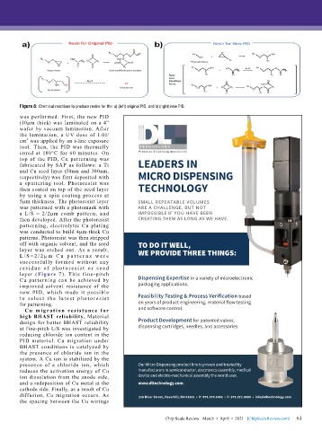
Figure 8: Chemical reactions to produce resins for the: a) (left) original PID, and b) (right) new PID.
        was performed. First, the new PID
        (10µm thick) was laminated on a 4”
        wafer by vacuum lamination. After
        the lamination, a UV dose of 1.0J/
           2
        cm  was applied by an i-line exposure
        tool. Then, the PID was thermally
        cured at 180°C for 60 minutes. On
        top of the PID, Cu patterning was
        fabricated by SAP as follows: a Ti         LEADERS IN
        and Cu seed layer (50nm and 300nm,
        respectively) was first deposited with     MICRO DISPENSING
        a sputtering tool. Photoresist was
        then coated on top of the seed layer       TECHNOLOGY
        by  using  a  spin  coating  process  at
        5µm thickness. The photoresist layer       SMALL REPEATABLE VOLUMES
        was patterned with a photomask with        ARE A CHALLENGE, BUT NOT
        a L/S = 2/2µm comb pattern, and            IMPOSSIBLE IF YOU HAVE BEEN
        then developed. After the photoresist      CREATING THEM AS LONG AS WE HAVE.
        patterning, electrolytic Cu plating
        was conducted to build 4µm-thick Cu
        patterns. Photoresist was then stripped
        off with organic solvent, and the seed     TO DO IT WELL,
        layer was etched out. As a result,         WE PROVIDE THREE THINGS:
        L / S = 2 /2 µ m C u p a t t e r n s w e r e
        successf ully for med without any
        r e s i d u e  of p ho t o r e s i s t  o r s e e d
        layer (Figure 7). This f ine-pitch
        Cu patterning can be achieved by           Dispensing Expertise in a variety of microelectronic
        improved solvent resistance of the         packaging applications.
        new PID, which made it possible
        t o s ele c t t h e l a t e s t pho t o r e si s t   Feasibility Testing & Process Verification based
        for patterning.                            on years of product engineering, material flow testing
          C u m i g r at i on  r e s i s t a nc e for   and software control.
        high BHAST reliability. Material
        design for better BHAST reliability        Product Development for patented valves,
        at fine-pitch L/S was investigated by      dispensing cartridges, needles, and accessories.
        reducing chloride ion content in the
        PID material. Cu migration under
        BHAST conditions is catalyzed by
        the presence of chloride ion in the
        system. A Cu ion is stabilized by the
        presence of a chloride ion, which          Our Micro Dispensing product line is proven and trusted by
        reduces the activation energy of Cu        manufacturers in semiconductor, electronics assembly, medical
        ion dissolution from the anode side,       device and electro-mechanical assembly the world over.
        and a redeposition of Cu metal at the      www.dltechnology.com.
        cathode side. Finally, as a result of Cu
        diffusion, Cu migration occurs. As         216 River Street, Haverhill, MA 01832  •  P: 978.374.6451  •  F: 978.372.4889  •  info@dltechnology.com
        the spacing between the Cu wirings


                                                                                                             61
                                                             Chip Scale Review   March  •  April  •  2021   [ChipScaleReview.com]  61

