Page 60 - ChipScale_Mar-Apr_2021-digital
P. 60
Hi-resolution dry-film PID material for high-density packaging


        By Yuya Suzuki, Chihiro Funakoshi, Daisuke Shibata, Daichi Okamoto, Yoko Shibasaki  [Taiyo Ink Mfg. Co.., Ltd.]
        T        his paper reports a new dry-  technology. Also, the PID


                 film type photo-imageable
                 dielectric (PID) material for   has high tensile strength
                                           and elongation, which
        fine-pitch and high-density multi-layer   are beneficial for high
        RDL structuring. High-density packaging   resistance to mechanical
        technologies are substantially required for   stresses— especially
        high-speed signal transmission in a variety   when it is applied for a
        of applications, such as high-performance   multi-layer RDL.
        computing, artificial intelligence (AI),   T h i s p a p e r f i r s t
        and 5G communications. To achieve high   describes the benefits
        functionality, new integrated circuit (IC)   and  challenges  of  our   Table 1: Material properties of a new PID.
        packaging technologies including fan-  previous generation PID
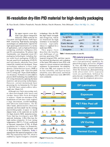
        out wafer-level packaging (FOWLP),   material (original PID), and then reports   PID material processing
        fan-out panel-level packaging (FOPLP),   the technical development and evaluation   PID materials are organic dielectrics
        and high-density substrates have been   of the latest PID material (new PID) with   with fine-patterning capability by
        intensively studied and developed. These   respect to solvent resistance and dielectric   photolithography  processes  (Figure
        technologies endeavor to have high-  resistance. To demonstrate  the reliability   1). First, the PID is laminated on base
        density redistribution layers (RDLs)   of the new PID, test coupons for line-  substrate layers by vacuum lamination.
        for signal routing with <5µm fine-pitch    to-line reliability and layer-to-layer   After the lamination, photopatterning
        L/S Cu wiring and <10µm small interlayer   reliability were fabricated, and biased   w it h u lt r av iolet ( U V ) ex p os u r e
        via structures. Evolution in semi-additive   highly-accelerated stress tests (BHAST)   tools are perfor med, followed by
        process (SAP) technology has enabled 2µm   were conducted.            polyethylene terephthalate (PET) film
        L/S wiring formation by applying the latest                           removal and development processes.
        materials and processing technologies.
        However, current mainstream laser
        processing for via formation by CO 2  laser
        or Nd-YAG laser cannot achieve ultra-
        small vias <10µm [1,2].
          Although new laser processing such
        as short-wavelength solid lasers and
        excimer lasers have been developed
        to achieve <10µm via structures [3,4],
        installation of new laser tools requires
        a large investment, careful handling,
        and laborious maintenance. On the
        other hand, photosensitive dielectric
        materials can form small vias by existing
        photolithography stepper or mask
        aligner tools, so the materials are useful
        for high-density RDL manufacturing.
        Taiyo Ink has developed a new PID
        material, featuring: 1) Dry-film type for
        high surface planarity; 2) Low curing
        temperature (180°C); 3) Low coefficient
        of thermal expansion (CTE); 4) High
        resolution for 6-10µm via formation;
        5) Resistance to organic solvents; and
        6) High dielectric reliability. Table 1
        summarizes the material properties of the
        PID. The material has low CTE, which is
        enabled by organic-inorganic composite
                                           Figure 1: Process flow of PID patterning.

        58
        58   Chip Scale Review   March  •  April  •  2021   [ChipScaleReview.com]

