Page 55 - ChipScale_Mar-Apr_2021-digital
P. 55
Effects of FOPLP layouts on large-area thermal chucks


        By Debbie Claire Sanchez, Klemens Reitinger, Sophia Oldeide, Wenxuan Song  [ERS electronic GmbH]
        C         omplexities in integrated                                   (KGDs) from a sawn silicon wafer, then


                  circuit (IC) applications
                  a n d t h e  d r i v e  t o w a r d                         placing them onto a temporary carrier
                                                                              laminated with thermal sensitive tape.
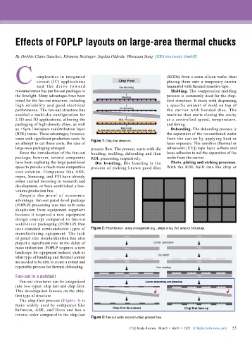
        miniaturization has put fan-out packages in                             Molding. The compression molding
        the limelight. Many advantages have been                              process is commonly used for the chip-
        noted for the fan-out structure, including                            first structure. It starts with dispensing
        high reliability and good electrical                                  a specific amount of mold on top of
        performance. The fan-out structure has                                the  carrier with  bonded dies. The
        enabled a multi-die configuration for                                 machine then starts closing the cavity
        2.5D and 3D applications, allowing the                                at a controlled speed, temperature,
        packaging of high-density chips, as well                              and timing.
        as <5µm line/space redistribution layer                                 Debonding. The debonding process is
        (RDL) traces. These advantages, however,                              the separation of the reconstituted wafer
        came with significant production costs. In                            from the carrier by applying heat or
        an attempt to cut these costs, the idea of   Figure 1: Chip-first structure.  laser exposure. The sensitive (thermal or
        large-area packaging emerged.      process flow. The process starts with die   ultraviolet [UV]) tape layer softens and
          Since the introduction of the fan-out   bonding, molding, debonding and then   loses adhesion to aid the separation of the
        package, however, several companies   RDL processing, respectively.   wafer from the carrier.
        have been exploring the large panel-level   Die bonding. Die bonding is the   Photo, plating and etching processes.
        space to provide a much more competitive   process of picking known good dies   With the RDL built into the chip or
        cost  solution.  Companies  like  ASE,
        nepes, Samsung, and PTI have already
        either started investing in research and
        development, or have established a low-
        volume production line.
          Despite the proof of economic
        advantage, fan-out panel-level package
        (FOPLP) processing was met with some
        skepticism from equipment suppliers
        because it required a new equipment
        design concept compared to fan-out
        wafer-level packaging (FOWLP) that
        uses standard semiconductor types of   Figure 2: Panel format - array arrangement (e.g., single array, 2x2 array or 3x3 array).
        manufacturing equipment. The lack
        of panel size standardization has also
        played a significant role in the delay of
        mass utilization. FOPLP requires a new
        landscape for equipment makers, such as
        what type of handling and thermal control
        are needed to be able to create a robust and
        repeatable process for thermal debonding.

        Fan-out in a nutshell
          Fan-out structures can be categorized
        into two types: chip last and chip first.
        This investigation focuses on the chip-
        first type of structure.
          The chip-first process (Figure 1) is
        more widely used by companies like
        Infineon, ASE, and Deca and has a
        reverse order compared to the chip-last
                                           Figure 3: Fan-out wafer reconstruction process flow.

                                                                                                             53
                                                             Chip Scale Review   March  •  April  •  2021   [ChipScaleReview.com]  53

