Page 52 - ChipScale_Mar-Apr_2021-digital
P. 52
t e s t i ng. Cr o s s - s e c t io n a n a ly si s
        provides further information about the
        resulting shape of the adhesive and its
        dependence on the process parameters.
          In  Table 1, the variations under
        a nalysis a re  g iven.  T he st a ndby
        temperature of the wafer was kept
        constant at 50°C. The main parameters
        under analysis are the chip temperature
        and the bonding pressure. After pick-
        up, a delay of 10s is applied so that
        the die is able to reach a homogeneous
        t e m p e r a t u r e  d i s t r i b ut i o n .  T h e
        temperature set points under analysis
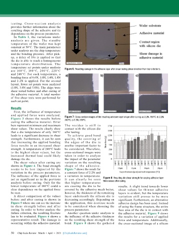
        are 160°C, 180°C, 200°C, 220°C     Figure 6: Resulting damage in the adhesive layer after shear testing (shear direction from top to bottom).
        and 240°C. For each temperature, a
        bonding force of 0.6N, 1.0N, 1.4N, 1.8N
        and 2.2N is applied. For the second
        layout, fewer set points were analyzed
        (1.0N, 3.0N and 5.0N). The chips were
        shear tested before and after curing of
        the adhesive material. A total number
        of five shear tests were performed for
        each set point.

        Results
          First, the influence of temperature
        and applied force were analyzed.
        Figure 3 shows the results before   Figure 7: Cross-section images of the resulting adhesive layer shape after curing: a) 2.2N, 180ºC; b) 2.2N,
                                           200ºC; c) 2.2N, 220ºC.
        curing the  adhesive material.  Error
        bars represent minimum and maximum   T h e r e s i d u e i s s t i l l i n
        shear values. The results clearly show   contact with the silicon die
        that a die temperature of only 160°C   after testing.
        leads to a significant decrease in shear   To achieve good bond
        strength. Furthermore, it can be seen   quality, the covering  of
        that increasing the applied bonding   t he e dge s of t he d ie is
        force results in an increased shear   another important factor to
        strength. A temperature of 240°C leads   be  considered.  Therefore,
        to the highest shear values, but the   cross-sectional images were
        increased thermal load could likely   taken in order to analyze
        damage the die.                    the impact of the parameter
          The shear values after curing are   variation on the resulting
        shown in Figure 4. The bond strength   s h a p e of t h e a d h e sive.
        seems to be less impacted by the   Figure 7 shows the result for
        variation in the process parameters.   a constant force of 2.2N and
        The influence of the applied force is   a variation in temperature.
        not as significant as in the previous   I t c a n c l e a r l y b e s e e n   Figure 8: Resulting die shear strength for varying adhesive layer
        analysis before curing. Only for the   that higher temperatures   thicknesses after curing.
        lowest temperature of 180°C could a   are causing the die to be       results. A slight trend towards lower
        clear dependency on the applied force   covered by the adhesive much better,   shear values for thinner adhesive
        be seen.                           however, the thickness of the remaining   layers is evident, but the temperature
          A direct comparison of the values   layer underneath the silicon die is   variation still proves to be more
        before and after curing is shown in   decreasing accordingly. Depending on   significant. Furthermore, an alternative
        Figure 5 where one can see the increase   the application, this decrease needs   adhesive design has been used. Instead
        in shear strength before and after   to be considered when choosing the   of using the frame structure, the entire
        curing. In order to better analyze the   process parameters.          face area of the die is in contact with
        failure criterion, the resulting fracture   Another question under analysis is   the adhesive material. Figure 9 shows
        has to be evaluated. Figure 6 shows a   the influence of the adhesive thickness   the results for a variation of applied
        representative result. The damage is   on the resulting shear strength of the   force and temperature. Additionally,
        occurring within the adhesive material.   bond.  Figure 8 shows the gathered   the cross-sectional image of a silicon


        50   Chip Scale Review   March  •  April  •  2021   [ChipScaleReview.com]
        50

