Page 50 - ChipScale_Mar-Apr_2021-digital
P. 50
Silicon die bonding using a photostructurable


        adhesive material


        By Kai Hollstein, Kirsten Weide-Zaage  [Institute for Microelectronic Systems, RESRI Workgroup]
        T        his article addresses the   commonly applied in order to build   lithographically-structured SU-8 on


                 usage of a photostructurable
                 a d h e s i v e  m a t e r i a l  f o r   microchannel systems. The following   top. The resist has a thickness of 30µm
                                           literature provides an overview with
                                                                              and a minimum structure size of 5µm.
        bonding a silicon chip onto a wafer   respect to thin adhesive layers used in   The paper addresses the inf luence
        s u r fa c e. Such a p ro c e s s st e p i s   wafer-to-wafer or substrate-to-wafer   of pressure and bonding time on the
        needed for a packaging technology   bonding applications.             bond quality, which is evaluated
        currently  under development.  The   I n [ 1 ] , a ph o t o s e n s i t i v e   using  microscopy  and  pull  tests.
        process under analysis demands that   benzocyclobutene dielectric (BCB)   Furthermore, the authors showed that
        a silicon chip be bonded face down   is used to bond together a glass
        onto a wafer substrate (Figure 1).   wafer  and  a  silicon  wafer.  The
                                           resulting compound is analyzed
                                           using wedge-opening test and
                                           tensile methods. The successful
                                           implementation is shown for
                                           applications in RF system design
                                           and a microfluidics system.
                                             In [2] and [3], a BCB material
                                           i s u s e d fo r a n ovel si l ic o n
                                           photonic build-up. Here, a III-V
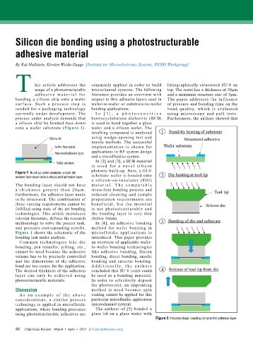
        Figure 1: Build-up under analysis: silicon die   substrate wafer is bonded onto
        bonded face down onto a structured adhesive layer.
                                           a silicon-on-insulator (SOI)
        The bonding layer should not have   m a t e r i a l.  T h e c o m p a r a b l e
        a t h ick ne s s g r e at e r t h a n 20 µ m .   stress-free bonding process and
        Furthermore, the adhesive layer needs   reduced cleaning and sample
        to be structured. The combination of   preparation requirements are
        these varying requirements cannot be   benef icial, but t he mater ial
        fulfilled using state of the art bonding   is not photostr ucturable and
        technologies. This article introduces   the bonding layer is very thin
        relevant literature, defines the research   (below 50nm).
        methodology to solve the project task,   In [4], an adhesive bonding
        and presents corresponding results.   method for wafer bonding in
        Figure 1 shows the schematic of the   microf luidic applications is
        bonding task under analysis.       introduced. This paper provides
          Com mon tech nologies li ke die   an overview of applicable wafer-
        bonding, pin transfer, jetting, etc.,   to-wafer bonding technologies
        cannot be used because the adhesive   like adhesive bonding, fusion
        volume has to be precisely controlled   bonding, direct bonding, anodic
        and the dimensions of the adhesive   bonding and eutectic bonding.
        bond are too coarse for the application.   A d d i t i o n a l l y, t h e a u t ho r s
        The desired thickness of the adhesion   concluded that SU-8 resist could
        layer can only be achieved using   be used as a bonding material.
        photostructurable materials.       In order to selectively deposit
                                           the photoresist, an imprinting
        Discussion                         method is used because spin
          A s a n e x a m p l e o f t h e a b o v e   coating cannot be applied for this
        considerations, a similar process   particular microfluidic application
        technology is applied in microfluidic   (microchannel system).
        applications, where bonding processes   The authors of  [5]  bonded a
        using photostructurable adhesives are   glass lid on a glass wafer with
                                                                         Figure 2: Process chain: bonding die onto the adhesive layer.

        48   Chip Scale Review   March  •  April  •  2021   [ChipScaleReview.com]
        48

