Page 46 - ChipScale_Mar-Apr_2021-digital
P. 46
Estimating BGA reliability of 2.5D packages using


        coupled thermal-mechanical simulation


        By Manish Nayini, Janak Patel  [Marvell Semiconductor]  Timothy Horn, Lloyd Burrell  [GLOBALFOUNDRIES]
        S        ilicon interposer technology,   etc. The JEDEC TC-J test is considered   with reticle stitched interposer, reticle


                 or 2.5D, is a type of system-
                                           thermal cycling fatigue reliability of
                 in-package (SiP) that provides   an industry standard test to evaluate   size application-specific integrated circuit
                                                                              (ASIC) and two HBMs, is detailed. Two
        an  opportunity to  integrate several   BGA solder balls. The test is a uniform   configurations are evaluated in this
        heterogeneous integrated circuit (IC)   temperature cycling with a fixed profile   test: with and without heat sink. The
        devices in the same package. Placing   and the test results need to be bridged   data collected from these tests are used
        multiple IC chips next to each other on   to the field application case. Therefore,   to validate the FEM simulation of the
        a passive silicon interposer allows for   there is a need to model and predict   thermal cycling. The coupled thermal-
                                               nd
        short and dense interconnection between   the 2  level interconnect reliability for   mechanical simulation technique is then
        the chips. This configuration enables   different applications.       used to predict BGA lifetime in field-like
        lower power, lower latency and higher   Several papers in previous literature   cycling conditions using the TC-J thermal
        bandwidth compared to traditional 2D   have evaluated BGA solder joint   cycling lifetime as a reference.
        packages [1]. 2.5D technology is seen   reliability in both thermal and power
        as an important solution to overcome   cycling using finite element modeling   TC-J reliability test
        limitations of Moore’s Law scaling and   (FEM). S. Shao, et al., [2] reported on a   The reliability test boards are designed
        finds use in several high-performance   parametric study of 2.5D package board-  as a 20 plus layer, 10” x 8”, 147.2mil-
        applications such as networking, graphics,   level reliability in thermal and power   thick, copper metal and FR-4 dielectric
        artificial intelligence (AI)/machine   cycling using combined computational   build-up layers with non-solder mask
        learning, etc. 2.5D packages consisting   fluid dynamic (CFD)-structural modeling.   defined (NSMD) pads. For monitoring
        of logic die and high-bandwidth memory   J. Wang et al., [3] discussed the effects of   of high-risk connections in the board,
        (HBM) stacked die are one of the most   package geometry and material properties   electrical connections are made to a 540-
        common configurations to increase the   on board-level solder joint reliability of   pin connector (interval measurement
        performance of the logic die.      a 2.5D package in accelerated thermal   only) and a 4-pin connector (in situ
                                           cycling. Various authors, such as B.   measurement only). In situ measurements
        Motivation                         Rodgers, et al., [4], L. Yin, et al., [5]   are the primary focus of this study
          With the increasing bandwidth    have investigated thermal cycling and   because of their capability to sense the
        requirements,  the  logic  die  size,   power cycling using coupled thermal-  exact time to fail under stress, enabling
        number of HBMs and, by extension,
        interposer size, organic laminate size,
        are increasing. This has necessitated
        the move to low coefficient of thermal
        expansion (CTE) organic laminates to
        improve the package coplanarity and
        also maintain ultra low-k (ULK) layer,
        underfill, and C4/micro-pillar reliability.
        However, this move to low CTE organic   Figure 1: Package, PCB and heat sink assembly.
        laminates results in an increased CTE
        mismatch between the package and   mechanical modeling techniques. Few   more precise estimation of the BGA life.
        conventional FR4 printed circuit board   papers such as those by L. Garner, et al.,   2.5D packages joined to the test boards
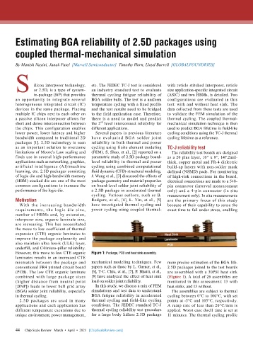
        (PCB). The low CTE organic laminate   [6], T-C. Chiu, et al., [7], P. Bhatti, et al.,   are assembled with a 30PSI heat sink
        combined with large package sizes   [8] have analyzed the effect of heat sink   (Figure 1). A total of 26 assemblies are
        (higher distance from neutral point   load on solder joint reliability.  monitored in this assessment: 13 with
        [DNP]) leads to lower ball grid array   In this study, we discuss a mix of FEM   heat sinks, and 13 without.
        (BGA) solder joint reliability, especially   simulations and test data to understand   The assemblies are subject to thermal
        in thermal cycling.                BGA fatigue reliability in accelerated   cycling between 0°C to 100°C, with set
          2.5D packages are  used  in many   thermal cycling and field-like cycling   points at -5°C and 105°C, respectively.
        applications and each application has   conditions. The JEDEC standard TC-J   A ramp rate of less than 20°C/min is
        different temperature excursions due to   thermal cycling reliability test procedure   applied. Worst case dwell time is set at
        unique environment, power management,   for a large body lidless 2.5D package   11 minutes. The thermal cycling profile


        44
        44   Chip Scale Review   March  •  April  •  2021   [ChipScaleReview.com]

