Page 51 - ChipScale_Mar-Apr_2021-digital
P. 51
using a reactive ion etch (RIE) plasma clean is not beneficial for bond
        quality. The process is used for a microfluidic system.
          In  [6],  several  photostructurable  materials  for  wafer-to-wafer
        bonding are compared. The underlying chemistry of the materials is
        either epoxy-based, siloxane-based, phenol-based or acrylic-based.
        The authors needed materials with a curing temperature below 250°C,
        so using BCB or a polyimide was not an option. In this study, a glass
        wafer and a silicon wafer were bonded to each other. The result was
        analyzed using optical microscopy and scanning electron microscopy
        (SEM) imaging. Thermogravimetric analysis was used to assess the
        thermal stability of the materials and Fourier transform infrared
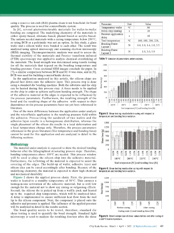
        (FTIR) spectroscopy was applied to analyze chemical crosslinking of  Table 1: Variation of parameters under analysis.
        the materials. The bond strength was determined using tensile testing
        for all the materials that depend on the bonding temperature and
        bonding pressure. Cross-sectional SEM images conclude the paper. In
        [7], a similar comparison between BCB and SU-8 was done, and in [8],
        BCB was used for building a microfluidic device.
          In the application analyzed in this article, the silicon chips are
        placed face down onto the adhesive layer. This process step is done
        using a standard die bonding machine. Both the substrate and the chip
        can be heated during this process step. A force needs to be applied
        on the chip in order to achieve sufficient bonding strength. The shape
        of the adhesive material at the edges is expected to be influenced by
        the process parameters. Furthermore, the resulting strength of the
        bond and the resulting shape of the adhesive  with respect to their
        dependence on the process parameters have not yet been referenced in
        literature.
          One of the main differences between the application under analysis
        and the microfluidic application is the resulting pressure field within   Figure 3: Shear testing results before curing with respect to
        the  adhesive.  Pressurizing  the  sandwich  of  two  wafers  and  the   temperature and bonding force variation.
        adhesive layer results in a homogeneous distribution, whereas the
        single placement of the silicon die results in a local deformation and
        a local temperature change only. Therefore, the process parameters
        referenced in the given literature (like temperature and bonding force)
        cannot be used for this application and are analyzed in detail in the
        following sections.

        Methodology
          The material under analysis is expected to show the desired bonding
        behavior after the lithographical structuring process steps. Therefore,
        bonding temperatures above 150°C are needed. This process window
        will be used to place the silicon chip into the adhesive material.
        Furthermore, the reflowing of the material is expected to assist the
        covering of the edges. The build-up of wafer, adhesive layer and
        silicon dies can be cured accordingly after bonding. Because of the   Figure 4: Shear testing results after curing with respect to
        underlying chemistry, the material is expected to show high chemical  temperature and bonding force variation.
        and mechanical durability.
          Figure 2 shows the applied process chain. First, the processed
        wafer is heated to a standby temperature of 50°C. This ensures a
        homogeneous activation of the adhesive material, but is still low
        enough for the material not to show any curing or outgassing effects.
        Second, the silicon die is picked up from a waffle pack and heated
        up to the  required chip temperature, which will be analyzed later.
        A delay is implemented to ensure sufficient heat flow from the tool
        tip to the silicon component. Next, the component is placed onto the
        adhesive and pressure is applied. The influence of the applied pressure
        will be analyzed in detail in the results section.
          The  bond  quality  needs  to  be  tested,  therefore,  standard  die
        shear testing is used to quantify the bond strength. Standard light
        microscopy is used to analyze the resulting fracture after die shear   Figure 5: Direct comparison of shear values before and after curing at
                                                                    a 220°C tool temperature.

                                                                                                             49
                                                             Chip Scale Review   March  •  April  •  2021   [ChipScaleReview.com]  49

