Page 56 - ChipScale_Mar-Apr_2021-digital
P. 56
shape (smiling or frowning). The warpage
                                                                              profiles change depending on several
                                                                              factors such as silicon to mold density, die
                                                                              shape (i.e., square and rectangular), number
                                                                              of RDLs, and specifically for the panel
                                                                              format, the chip layout plays a significant
                                                                              factor (Figure 2).


        Figure 4: Thermal shot illustrating heat dissipation when a high-temperature wafer is in contact with a low-
        temperature object.


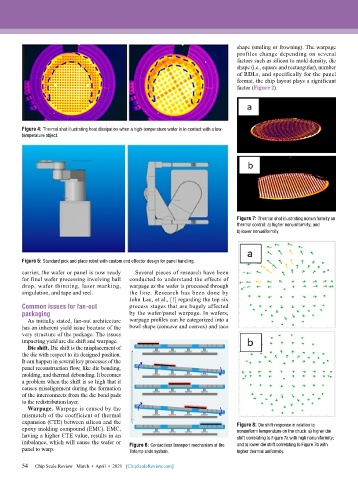
                                                                              Figure 7: Thermal shot illustrating nonuniformity on
                                                                              thermal control: a) higher nonuniformity; and
                                                                              b) lower nonuniformity.


        Figure 5: Standard pick and place robot with custom end effector design for panel handling.
        carrier, the wafer or panel is now ready   Several pieces of research have been
        for final wafer processing involving ball   conducted to understand the effects of
        drop, wafer thinning, laser marking,   warpage as the wafer is processed through
        singulation, and tape and reel.    the line. Research has been done by
                                           John Lau, et al., [1] regarding the top six
        Common issues for fan-out          process stages that are hugely affected
        packaging                          by the wafer/panel warpage. In wafers,
          As initially stated, fan-out architecture   warpage profiles can be categorized into a
        has an inherent yield issue because of the   bowl shape (concave and convex) and taco
        very structure of the package. The issues
        impacting yield are die shift and warpage.
          Die shift. Die shift is the misplacement of
        the die with respect to its designed position.
        It can happen in several key processes of the
        panel reconstruction flow, like die bonding,
        molding, and thermal debonding. It becomes
        a problem when the shift is so high that it
        causes misalignment during the formation
        of the interconnects from the die bond pads
        to the redistribution layer.
          Warpage. Warpage is caused by the
        mismatch of the coefficient of thermal
        expansion (CTE) between silicon and the
        epoxy molding compound (EMC). EMC,                                    Figure 8: Die shift response in relation to
                                                                              nonuniform temperature on the chuck: a) higher die
        having a higher CTE value, results in an                              shift correlating to Figure 7a with high nonuniformity;
        imbalance, which will cause the wafer or                              and b) lower die shift correlating to Figure 7b with
        panel to warp.                     Figure 6: Contactless transport mechanism of the   higher thermal uniformity.
                                           Tritemp slide system.
        54
        54   Chip Scale Review   March  •  April  •  2021   [ChipScaleReview.com]

