Page 61 - ChipScale_Mar-Apr_2021-digital
P. 61
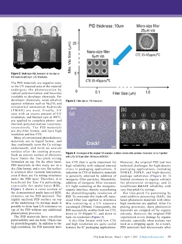
Figure 2: Multi-layer RDL formation in the original
        PID example with 4µm L/S/ structures.
        The PID materials are negative tone,
        so the UV exposed area of the material
        u nde rgoe s t he phot ore a ct ion by
        radical polymerization and becomes
        insoluble to developer chemicals. For
        developer chemicals, weak alkaline   Figure 3: Filler size vs. PID resolution.
        aqueous solutions such as Na 2 CO 3  and
        tetramethyl ammonium hydroxide
        ( T M A H ) a r e u s e d . Fi n a l ly, U V
        cure with an excess amount of UV
        irradiation, and thermal cure at 180°C,
        are applied to complete photo- and
        thermal-polymerization reactions,
        respect ively.  T he  PI D  mater ials
        are dry-film format, and have high
        resolution and low CTE.
          Many of conventional photodielectric
        materials are in liquid format, and
        they conformally cover the Cu wirings
        u nder neath, and for m an u neven
        surface after the coating process.
        Such an uneven surface of dielectric   Figure 4: Challenges of the original PID example: a) Micro-cracks after acetone immersion; b) Cu migration
        layer limits the fine-pitch wiring   with L/S=10/10µm after 100 hours of BHAST.
        formation on top. On the other hand,   low CTE that is quite important for   However, the original PID had two
        PID materials in this study are in a   high reliability with reduced internal   technical challenges for high-density
        dry-film format, and a very flat surface   stress in packaging applications. A   packaging applications, including
        is attained after vacuum lamination,   reduction in CTE of dielectric materials   FOWLP, FOPLP, and high-density
        even if there are Cu wiring structures   is generally attained by addition of   package substrates (Figure 4): 1)
        under the PID layer. Therefore, it is   inorganic filler particles. Meanwhile,   limited resistance to organic solvents
        beneficial for fine-Cu patterning,   addition of inorganic filler increases   for photoresist st r ipping; and 2)
        especially for mu lt i-layer R DL.   UV light scattering at the inorganic-  insufficient BHAST reliability with
        Figure 2 shows a cross section of   organic interface, thereby exacerbating   very fine-pitch Cu wirings.
        the demonstrated multi-layered RDL   the photolithography resolution of   For fine-pitch Cu patterning by
        structure on the PID material. The   PID. To overcome this trade-off, nano-  semi-additive processing (SAP), the
        highly uniform PID surface on top   sized filler was applied to minimize   latest photoresist materials with ultra-
        of the underlying Cu wirings made it   Mie scattering at a UV exposure   high resolution are applied. After Cu
        possible to form 4µm L/S structures on   wavelength (365nm). Consequently, the   plating processes, these photoresist
        top of the PID without any additional   PID successfully enables both low CTE   materials are stripped off by organic
        planarization processes.           down to 35-45ppm/°C, and down to   solvents. However, the original PID
          The PID materials have excellent   6µm via resolution (Figure 3).   experienced severe damage by organic
        patternability and can form <10µm vias   A dry-film format with low CTE   solvents, especially when acetone was
        by photolithography. In addition to the   and high resolution are quite useful   used as a stripping agent. As a result,
        high resolution, the PID materials have   features for IC packaging applications.   PID materials had microcracks after


                                                                                                             59
                                                             Chip Scale Review   March  •  April  •  2021   [ChipScaleReview.com]  59

