Page 53 - ChipScale_Mar-Apr_2021-digital
P. 53
application. Literat u re
                                                     h a s b e e n c i t e d w i t h
                                                     comparable  applications
                                                     mainly in microf luidics.
                                                     The available literature is
                                                     not showing any application
                                                     of these technologies for
                                                     silicon die fixation on a
                                                     wafer substrate. The work
                                                     discussed in this article
                                                     has shown the eff icacy
                                                     of the photostructurable
                                                     adhesive for the application
                                                     under analysis. Bonding
                                                     parameters and adhesive
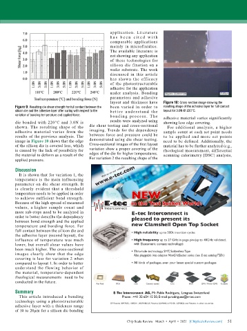
                                                     layout and thickness have   Figure 10: Cross-section image showing the
        Figure 9: Resulting die shear strength for full contact between the   been varied in order to   resulting shape of the adhesive layer for full contact
        silicon die and the adhesive layer after curing with respect to the   b e t t e r  u nd e r s t a nd  t he   layout for 3.0N @ 220°C.
        variation of bonding temperature and applied force.  b o nd i n g  p r o c e s s.  T he   adhesive material varies significantly
        die bonded with 220°C and 3.0N is            results were analyzed using   showing less edge covering.
        shown. The resulting shape of the   die shear testing and cross-sectional   For additional analysis, a higher
        adhesive material varies from the   imaging. Trends for the dependency   sample count at each set point needs
        results of the previous analysis. The   between force and pressure could be   to  be  applied  and  more  set  points
        image in Figure 10 shows that the edge   demonstrated using die shear testing.   need to be defined. Additionally, the
        of the silicon die is covered less, which   Cross-sectional images of the first layout   material has to be further analyzed (e.g.,
        is caused by the lack of possibility for   variation show a proper covering of the   rheological measurement, differential
        the material to deform as a result of the   edges of the die for higher temperatures.   scanning calorimetry [DSC] analysis,
        applied pressure.                  For variation 2 the resulting shape of the

        Discussion
          It is shown that for variation 1, the
        temperature is the main influencing
        parameter on die shear strength. It
        is clearly evident that a threshold
        temperature needs to be applied in order
        to achieve sufficient bond strength.
        Because of the high spread of measured
        values, a higher sample count and
        more sub-steps need to be analyzed in
        order to better describe the dependency
        between bond strength and the applied
        temperature and bonding force. For
        full contact between the silicon die and
        the adhesive layer (second layout), the
        influence of temperature was much
        lower, but overall shear values have
        been much higher. The cross-sectional
        images clearly show that the edge
        covering is less for variation 2 when
        compared to layout 1. In order to better
        understand the flowing behavior of
        the material, temperature-dependent
        rheological measurements  need to be
        conducted in the future.

        Summary                                        E-Tec Interconnect  AG, Mr. Pablo Rodriguez,  Lengnau Switzerland
          This article introduced a bonding                Phone : +41 32 654 15 50, E-mail: p.rodriguez@e-tec.com
        technology using a photostructurable
        adhesive layer with a thickness range
        of 10 to 20µm for a silicon die bonding

                                                                                                             51
                                                             Chip Scale Review   March  •  April  •  2021   [ChipScaleReview.com]  51

