Page 14 - ChipScale_Mar-Apr_2021-digital
P. 14
silicon on insulator [FDSOI] 28nm node)   f r a m e w o r k , t h e t e a m j o i n t l y   two technological tracks, one being
        three-dimensionally stacked on an active   demonstrated world-class figures of   new integration schemes and processes
        silicon interposer (complementary metal-  merit, such as 3D network-on-chip   for reducing 3D interconnects pitch,
        oxide-semiconductor [CMOS] 65nm    (NOC) communications at 1.2GHz     and assembly technologies being the
        node). The work described technologies   while achieving up to 3Tbits/s/mm² in   other, CEA-Leti pursued a technology
        such as TSV-middle and die-to-die fine-  efficiency. As for power consumption,   roadmap that combines historical
        pitch interconnects (20µm).        the demonstration showed how an    techniques with newer options such as
          In 2020 at IEEE ISSCC [5], CEA-  astonishingly low 1.1W for 3.2Tb/s   direct hybrid bonding, in addition to
        Leti and its partners unveiled the   could be achieved. The work paves the   die-to-wafer approaches for reaching
        architecture of this HPC demonstration,   way for future high-efficiency systems   a die-to-die interconnect pitch of 5 to
        as well as its performance metrics   supporting HPC.                  10µm, or even lower.
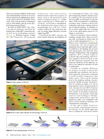
        (Figure 4). Working together within   Convinced  that HPC  systems can   CEA-Leti initiated a direct hybrid-
        t h e  I RT  N a no e l e c  3D p r o g r a m   fully benefit from the development of   bonding variant more than ten years
                                                                              ago, now well-known at wafer-scale, in
                                                                              a die-to-wafer integration [6] (Figure 5).
                                                                              What is now considered a mainstream
                                                                              tec h n o l o g y  f o r  h e te r o g en e o u s
                                                                              integration was at that time quite exotic.
                                                                              In addition to developing the process
                                                                              and integration, the institute also
                                                                              initiated collaboration with equipment
                                                                              suppliers. SET, a French leader in
                                                                              accurate flip-chip bonding, and CEA-
                                                                              Leti together demonstrated in the
                                                                              3D IRT Nanoelec program both the
                                                                              technical feasibility of the approach, as
                                                                              well as the industrial relevance of such
                                                                              an integration.
                                                                                Consider an example: Whatever
                                                                              its promise in terms of die-to-die
                                                                              bandwidth and reliability, the die-to-
                                                                              wafer approach, particularly compared
                                                                              to wafer-to-wafer integration, only
                                                                              makes sense if dies can be selected
                                                                              prior to the bonding, making a known-
        Figure 4: IntAct interposer. © CEA-Leti                               good-die (KGD) strategy mandatory.
                                                                              Even if evident on paper, it is not so
                                                                              plug-and-play from a practical point of
                                                                              view. Design-for-test (DFT) features
                                                                              are also required (demonstrated by
                                                                              CEA thanks to the IntAct interposer).
                                                                              Furthermore, test methods, classically
                                                                              used for wire bonding or thermo-
                                                                              compression interconnect, must be
                                                                              adapted in order to be compatible with
                                                                              direct hybrid bonding topology and
                                                                              contamination constraints.
                                                                                At t he end of 2020, CEA-Let i
                                                                              successfully demonstrated proof-
                                                                              of-concept for the KGD approach
                                                                              that is compatible with direct hybrid
        Figure 5: Die-to-wafer: make connection with 3D technology. © CEA-Leti


        Figure 6: The self-assembly principle. © CEA-Leti

        12   Chip Scale Review   March  •  April  •  2021   [ChipScaleReview.com]
        12

