Page 11 - ChipScale_Mar-Apr_2021-digital
P. 11

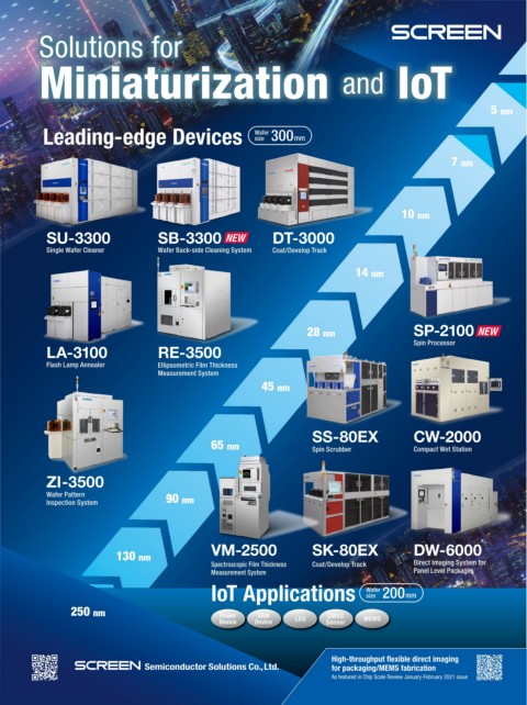
Solutions for
          S  ol  u   t io  ns     f o  r

          Miniaturization   IoT
                                                                             and


                                                                                                              5 nm
          Leading-edge Devices                            size 300 mm
                                                          Wafer


                                                                                                     7 nm


                                                                                          10 nm

           SU-3300                  SB-3300        NEW        DT-3000
           Single Wafer Cleaner     Wafer Back-side Cleaning System  Coat/Develop Track

                                                                                14 nm


                                                                     28 nm                   SP-2100 NEW
                                                                                             Spin Processor
           LA-3100                  RE-3500
           Flash Lamp Annealer      Ellipsometric Film Thickness
                                    Measurement System
                                                           45 nm


                                                                      SS-80EX                CW-2000
                                                65 nm                 Spin Scrubber          Compact Wet Station


           ZI-3500
           Wafer Pattern
           Inspection System          90 nm


                                                VM-2500               SK-80EX                DW-6000
                           130 nm
                                                Spectroscopic Film Thickness   Coat/Develop Track  Direct Imaging System for
                                                Measurement System                           Panel Level Packages
                                                IoT Applications                  size 200 mm
                                                                                  Wafer

                 250 nm                           Power   SAW             CMOS
                                                  Device  Device   LED   Sensor   MEMS


                                                                           High-throughput flexible direct imaging
                                                                           for packaging/MEMS fabrication
                                                                           As featured in Chip Scale Review January-February 2021 issue
   6   7   8   9   10   11   12   13   14   15   16