Page 10 - ChipScale_Mar-Apr_2021-digital
P. 10
Solutions for
                                                                                                                               S  ol  u   t io  ns     f o  r


                                                                                                                                                                                                  and
        Heterogeneous 3D integration for high-performance                                                                      Miniaturization   IoT


        computing                                                                                                                                                                                                                  5 nm


        By Séverine Chéramy, Emilie Bourjot  [CEA-Leti] Johanna M. Swan [Intel]                                                Leading-edge Devices                            size 300 mm
                                                                                                                                                                               Wafer
        F        ollowing  several  years  of   enhancement may be obtained through   organization took a different approach.                                                                                             7 nm


                 continuous  improvement
                                                                              of a multi-die interconnect bridge using
                                           leading to quicker time-to-market and
                 and massive R&D efforts by   power and area savings, as well as   They developed the first instantiation
        chipmakers and research organizations,   re-use of chiplets across a broader array   silicon within the package, now known
        supercomputers will soon reach exascale-  of application-specific microelectronic   as the embedded multi-die interconnect                                                                             10 nm
        level computing performance. Traditionally,   solutions (Figure 1).   bridge (EMIB) [1]. Using small bridge
        the ongoing increase in computing and                                 dies embedded as part of the substrate,           SU-3300                  SB-3300        NEW        DT-3000
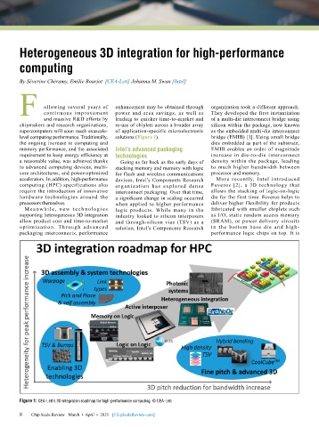
        memory performance, and the associated   Intel’s advanced packaging   EMIB enables an order of magnitude
        requirement to keep energy efficiency at   technologies               increase in die-to-die interconnect               Single Wafer Cleaner     Wafer Back-side Cleaning System  Coat/Develop Track
        a reasonable value, was achieved thanks   Going as far back as the early days of   density within the package, leading
        to advanced computing devices, multi-  stacking memory and memory with logic   to much  higher  bandwidth  between                                                                           14 nm
        core architectures, and power-optimized   for flash and wireless communications   processor and memory.
        accelerators. In addition, high-performance   devices, Intel’s Components Research   More recently, Intel introduced
        computing (HPC) specifications also   organization  has  explored  dense   Foveros [2], a 3D technology that
        require the introduction of innovative   interconnect packaging. Over that time,   allows the stacking of logic-on-logic
        hardware technologies around the   a significant change in scaling occurred   die for the first time. Foveros helps to
        processors themselves.             when applied to higher performance   deliver higher flexibility for products                                                                   28 nm                   SP-2100 NEW
          Me a nwh i le, new t e ch nolog ie s   logic products. While many in the   fabricated with smaller chiplets such                                                                                        Spin Processor
        supporting heterogeneous 3D integration   industry looked to silicon interposers   as I/O, static random access memory   LA-3100                 RE-3500
        allow product cost and time-to-market   and through-silicon vias (TSV) as a   (SRAM), or power delivery circuits        Flash Lamp Annealer      Ellipsometric Film Thickness
        optimization. Th rough advanced    solution, Intel’s Components Research   in the bottom base die and high-                                      Measurement System
        packaging interconnects, performance                                  performance logic chips on top. It is                                                             45 nm


                                                                                                                                                                                           SS-80EX                CW-2000
                                                                                                                                                                     65 nm                 Spin Scrubber          Compact Wet Station


                                                                                                                                ZI-3500
                                                                                                                                Wafer Pattern
                                                                                                                                Inspection System          90 nm


                                                                                                                                                                     VM-2500               SK-80EX                DW-6000
                                                                                                                                                130 nm
                                                                                                                                                                     Spectroscopic Film Thickness   Coat/Develop Track  Direct Imaging System for
                                                                                                                                                                     Measurement System                           Panel Level Packages
                                                                                                                                                                     IoT Applications                  size 200 mm
                                                                                                                                                                                                       Wafer

                                                                                                                                      250 nm                           Power   SAW             CMOS
                                                                                                                                                                       Device  Device   LED   Sensor   MEMS


        Figure 1: CEA-Leti’s 3D integration roadmap for high-performance computing. © CEA-Leti                                                                                                  High-throughput flexible direct imaging
                                                                                                                                                                                                for packaging/MEMS fabrication
                                                                                                                                                                                                As featured in Chip Scale Review January-February 2021 issue
        8 8  Chip Scale Review   March  •  April  •  2021   [ChipScaleReview.com]

