Page 18 - ChipScale_Mar-Apr_2021-digital
P. 18
Fan-out embedded bridge packaging for cost-effective


        chiplet integration


        By C. Key Chung, Shuai-Lin Liu, Jackson Li  [Siliconware Precision Industries Co., Ltd.]
        W            ith transistor scaling   by lowering the package cost, improving   Introduction


                     reaching both physical
                                                                                By now, Moore’s Law has clearly
                                           reliability performance. In this article,
                     and economic barriers,   the electrical signals, and having better   ended with respect to Si scaling [1], and
        transistor performance and cost have been   we present a demonstration of an FOEB   the role of advanced packaging to extend
        increasingly lagging behind the historical   test vehicle in which chips are integrated   this trend is of utmost importance. The
        Moore’s Law trajectory. However, demand   as follows: one application-specific   growth of semiconductors has been driven
        for silicon remains incessant with the   integrated circuit (ASIC) die and 4 high-  by the demands of smartphones and
        growth of transmission rate. Development   bandwidth memory (HBM) dies with four   tablets, but these markets are now slowing
        of electronic devices has increasingly   embedded bridge dies on a mold-based   down and being overtaken by high-
        required greater high-density package   interposer, and one layer of an RDL.   performance computing (HPC) and big
        integration. The electronic industry’s   The embedded bridge dies are fabricated   data computing (BDC). HPC and BDC
        response to this demand on package   using 65nm node technology with 0.56μm   demand very high-frequency and high-
        integration is to use chiplet-based devices   Cu line and space. By comparing the   speed transmission with lower latency,
        for improving yield and lowering the total   warpage of a 2.5D package with a similar   high-bandwidth and power efficiency
        cost. Chiplet packaging has now become   package size, we show that the FOEB chip   requirements. These requirements have
        a key technology to continue Moore’s   module has a similar warpage shape to the   created a different level of packaging
        Law. Intensive research has resulted in the   substrate, and the final package assembly   complexity and challenges. One solution
        development of multiple chiplet packages,   with the substrate—so the warpage value   to meet these demands is to integrate
        such as multi-chips on a Si interposer   is identical to the 2.5D package. Therefore,   multiple dies into an electronic package.
        using through-silicon via (TSV) (2.5D),   it has much lower stress residues as   These  packages  are  designed  either
        die-to-die stacked on each other (3D), fan-  compared to a 2.5D package.  Because of   homogeneously or heterogeneously
        out multi-chip module (FOMCM), and   this finding, the FOEB package has been   with integrated devices [2-4]. Over the
        embedded multi-die interconnect bridge   validated: it has a 2x longer temperature   years, electronic assembly houses have
        (EMIB). These packages were developed   cycle without a single failure as compared   developed a plethora of chiplet packages
        for the ser ver, high-perfor mance   to a 2.5D package. This finding allows   for multi-chip integration.
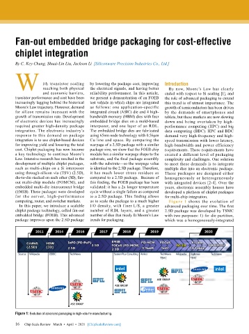
        computing, router, and switcher markets.   us to scale the package to a much higher   Figure 1 shows the evolution of
          In this paper, we introduce a scalable   I/O density, with finer L/S, a greater   advanced packaging over time. The first
        chiplet package technology, called fan-out   number of RDL layers, and a greater   2.5D package was developed by TSMC
        embedded bridge (FOEB). This advanced   number of dies that nicely fit Moore’s Law    with two purposes: 1) for die partition,
        package improves upon the 2.5D package   trends for packaging.        which was a homogeneously-integrated


        Figure 1: Evolution of advanced packaging in high-volume manufacturing.

        16
        16   Chip Scale Review   March  •  April  •  2021   [ChipScaleReview.com]

