Page 21 - ChipScale_Mar-Apr_2021-digital
P. 21
264hrs, and the high-temperature storage
                                                                              life (HTSL) test  (1000hrs) [13-19]. Owing
                                                                              to these reasons, the FOEB package has
                                                                              a great chance to supersede the 2.5D
                                                                              package as it has better design flexibility,
                                                                              scalability, and the benefit of a lower cost.
                                                                                One of the technologically certificated
                                                                              FOEB devices comprises 1 SoC +
                                                                              4HBM package structure with a package
                                                                                                  2
                                                                              dimension of 5,075mm  with a fan-out
                                                                                                  2
                                                                              module size of 1,250mm . The structure
                                                                              passed JEDEC standard reliability tests.
                                                                              The packages were first preconditioned
                                                                              using moisture soaking level 4 (MSL4)
                                                                              requirements, and then subsequently
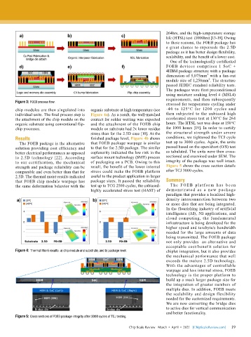
        Figure 3: FOEB process flow.
                                                                              stressed for temperature cycling under
        chip modules are then singulated into   organic substrate at high temperature (see   -40 to 125°C for 1200 cycles and
        individual units. The final process step is   Figure 4a). As a result, the well-matched   then subjected to the unbiased high
        the attachment of the chip module on the   contact for solder wetting was expected   accelerated stress test at 130°C for 264
        organic substrate using conventional flip-  and the attachment of the FOEB chip   hours. The HTSL test was done at 150°C
        chip processes.                    module on substrate had 2x lower residue   for 1000 hours [19]. In order to certify
                                           stress than for the 2.5D case [10]. At the   the structural strength under severe
        Results                            finished package level, Figure 4b shows   conditions, we tightened the TCJ cycle
          The FOEB package is the alternative   that FOEB package warpage is similar   test up to 3000 cycles. Again, the units
        solution providing cost efficiency and   to that for the 2.5D package. The similar   passed based on the open/short (O/S) test
        better electrical performances as opposed   coplanarity indicated the low risk in the   as tabulated. The units were then cross-
        to  2.5D technology [22]. According   surface mount technology (SMT) process   sectioned and examined under SEM. The
        to our certification, the mechanical   of packaging on a PCB. Owing to this   integrity of the package was well intact.
        strength and package reliability can be   result, the benefit of the lower internal   Figure 5 shows the cross section details
        comparable and even better than that for   stress could make the FOEB platform   after TCJ 3000 cycles.
        2.5D. The thermal moiré results indicated   useful to the product application in larger
        that FOEB chip module warpage has   package sizes. It passed the reliability   Summary
        the same deformation behavior with the   test up to TCG 2500 cycles, the unbiased-  T h e FOE B pl a t fo r m h a s b e e n
                                           highly accelerated stress test (HAST) of   de mon st r at e d a s a new pa ck age
                                                                              paradigm that provides a localized high-
                                                                              density interconnection between two
                                                                              or more dies that are being integrated.
                                                                              In the flourishing industry of artificial
                                                                              intelligence (AI), 5G applications, and
                                                                              cloud computing, the  fundamental
                                                                              infrastructure is being developed for the
                                                                              higher speed and terabyte/s bandwidth
                                                                              needed for the large amounts of data
                                                                              being transmitted. The FOEB package
                                                                              not only provides  an alternative and
                                                                              acceptable cost/benefit solution for
        Figure 4: Thermal Moiré results: a) chip module and substrate; and b) package level.  chiplet integration, but it also provides
                                                                              the mechanical performance that well
                                                                              exceeds the mature 2.5D technology.
                                                                              With the advantages of controllable
                                                                              warpage and less internal stress, FOEB
                                                                              technology is the proper platform to
                                                                              build up a much larger package size for
                                                                              the integration of greater numbers of
                                                                              multiple dies. In addition, FOEB meets
                                                                              the scalability and design flexibility
                                                                              needed for the customized requirements.
                                                                              We are now converting the bridge dies
                                                                              to active dies for vertical communication
                                                                              and better functionality.
        Figure 5: Cross sections of FOEB package integrity after 3000 cycles of TCJ testing.

                                                                                                             19
                                                             Chip Scale Review   March  •  April  •  2021   [ChipScaleReview.com]  19

