Page 24 - ChipScale_Mar-Apr_2021-digital
P. 24
Enabling wafer thinning using a glass carrier


        By Julia Brueckner, Andreas Gaab, Steven Lin, Erica Chang, Toshihiko Ono, Varun Singh, Jay Zhang  [Corning Incorporated]
        and Sebastian Tussing, Walter Spiess  [SÜSS MicroTec]
        W            afe r t h i n n i ng is a n


                     industry trend driven by
                     functional requirements
        or form factor considerations. For example,
        3D stacked memory uses silicon (Si) that
        is thinned to <50µm to enable through-
        silicon via (TSV) interconnection.
        Insulated-gate bipolar transistor (IGBT)
        chips rely on very thin wafers for vertical
        structural realization. Many components
        used for mobile devices are thinned before
        packaging to accommodate the height
        constraints imposed by design or aesthetics.
        When the final wafer thickness is greater
        than 100µm, backgrinding tapes are
        typically used to support the wafer during
        the thinning process. Thinning beyond this
        thickness often necessitates the use of a
        more rigid support, such as a carrier wafer.
          Wafer thinning is often accompanied
        by post-thinning processing that happens
        at elevated temperatures, e.g., metal or
        dielectric deposition. Differences in the
        coefficient of thermal expansion (CTE) of
        the carrier and that of the wafer can cause
        shape distortion, resulting in undesirable
        consequences such as lithography errors, or
        even wafer breakage. For convenience, we
        use the term warp in this article to describe
        shape distortion.
          An ideal carrier wafer for wafer thinning
        should have a CTE matched to that of the
        wafer to be thinned. In this article, we will
        also discuss other levers that may be used to
        minimize shape distortion during thinning
        and post-thinning processing.
          This article will explain why glass is
        an ideal carrier material. We will also
        demonstrate why glass carrier wafers are
        not only ideal for laser debonding, but that
        they can also be used with automated,
        mechanical debonding tools.

        What impacts wafer warp?
          We begin by first developing the
        fundamental understanding of what
        impacts wafer warp. In a previous article
        in this journal [1], we showed a simplified
        formula that can be used to estimate bi-
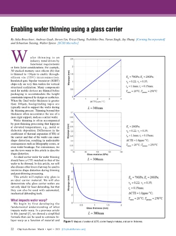
        layer warp as a function of material and   Figure 1: Warp as a function of ΔCTE, carrier Young’s modulus, and carrier thickness.


        22
        22   Chip Scale Review   March  •  April  •  2021   [ChipScaleReview.com]

