Page 27 - ChipScale_Mar-Apr_2021-digital
P. 27
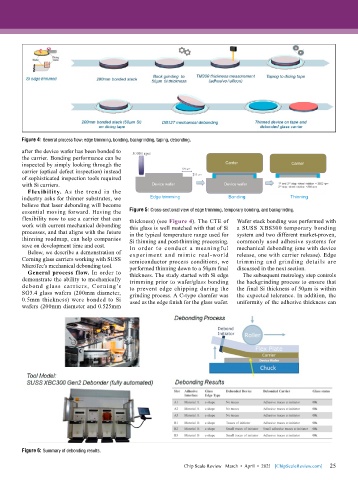
Figure 4: General process flow: edge trimming, bonding, backgrinding, taping, debonding.
        after the device wafer has been bonded to
        the carrier. Bonding performance can be
        inspected by simply looking through the
        carrier (optical defect inspection) instead
        of sophisticated inspection tools required
        with Si carriers.
          Flexibility.  As  the  trend  in  the
        industry asks for thinner substrates, we
        believe that laser debonding will become
        essential moving forward. Having the   Figure 5: Cross-sectional view of edge trimming, temporary bonding, and backgrinding.
        flexibility now to use a carrier that can   thickness) (see Figure 4). The CTE of   Wafer stack bonding was performed with
        work with current mechanical debonding   this glass is well matched with that of Si   a SUSS XBS300 temporary bonding
        processes, and that aligns with the future   in the typical temperature range used for   system and two different market-proven,
        thinning roadmap, can help companies   Si thinning and post-thinning processing.   commonly used adhesive systems for
        save on development time and cost.  In order to conduct a meaningful   mechanical debonding (one with device
          Below, we describe a demonstration of   experiment and mimic real-world   release, one with carrier release). Edge
        Corning glass carriers working with SUSS   semiconductor process conditions, we   trimming and grinding details are
        MicroTec’s mechanical debonding tool.  performed thinning down to a 50µm final   discussed in the next section.
          General process flow. In order to   thickness. The study started with Si edge   The subsequent metrology step controls
        demonstrate the ability to mechanically   trimming prior to wafer/glass bonding   the backgrinding process to ensure that
        debond glass car riers, Cor ning’s   to prevent edge chipping during the   the final Si thickness of 50µm is within
        SG3.4 glass wafers (200mm diameter,   grinding process. A C-type chamfer was   the expected tolerance. In addition, the
        0.5mm thickness) were bonded to Si   used as the edge finish for the glass wafer.   uniformity of the adhesive thickness can
        wafers (200mm diameter and 0.525mm


        Figure 6: Summary of debonding results.

                                                                                                             25
                                                             Chip Scale Review   March  •  April  •  2021   [ChipScaleReview.com]  25

