Page 32 - ChipScale_Mar-Apr_2021-digital
P. 32
tin to 18% increases the melting point to   heat as soon as possible. The bonding   process usually is a 5-10 cycle scrubbing
        350°C. The eutectic reflow temperature   force of the eutectic process may be set   movement under a certain amplitude and
        should be 20-40°C higher than the   to 30~100g. Scrubbing must be applied   frequency in X-Y-Z directions. During
        melting point. Because of reliability   during die attachment to eliminate voids.  the eutectic  process,  the scrubbing
        concerns, a maximum reflow temperature   Void-free processing. Solvent cleaning   process distributes the solder and
        of 320°C for a maximum of 30 seconds   of solder preforms and substrates/  removes the gas bubbles that are among
        is recommended for GaAs and GaN.   packages is recommended to remove   the main reasons for void generation.
        The temperature profile is dependent on   any existing surface contaminants (from   Epoxy process. The epoxy process
        the eutectic stage, the size and number   machining, packaging, handling, etc.).   has mostly been used for attaching
        of dies, and the substrate, etc. The first   GaAs and GaN can be cleaned using   passive components, such as capacitors,
        step of the process is to pick and place   an oxygen or plasma cleaning process   but not active components in RF PA
        the solder preform while at a pre-heating   before the eutectic process. During the   devices. In recent years, new adhesive
        temperature. The second step of the   eutectic process, an inert gas (nitrogen or   materials have been developed to replace
        process is to pick and place the die. The   nitrogen with 5-10% hydrogen) is used   AuSn. Silver micron-particle sintering
        die are placed on top of the solder preform   to surround the parts and remove oxygen   joining technology developed by Prof.
        either at the reflow temperature, or just   during reflow, preventing oxidation of the   Katsuaki Suganuma of Osaka University
        before reaching it. The die are placed with   interconnect surface.   has enabled pressureless die bonding
        a force of 10~100g and scrubbed according   Reliable eutectic die attach of high-  in ambient temperature at a low cost.
        to some preprogrammed parameters. In   power/high-frequency devices requires   Because this technology showed high
        some cases, the preform is pre-deposited   nearly a void-free attachment. A   reliability at high temperatures over
        on either the substrate or the PA chip.  better than 95% void-free attachment   250°C, its use is spreading as a key next-
          LDMOS eutectic process. AuSi is   is achievable with a scrub assist. An   generation power semiconductor die
        used for ultra-high thermal demand   oxygen level >10,000ppm contributes to   bonding technology. There is a lot of
        applications, such as silicon-based   voiding poor quality solder joints. The   ongoing research and development work
        LDMOS. The packaging or substrate   oxygen level in the eutectic chamber of   on the pressureless nano Ag sintering
        materials of LDMOS RF PA devices are   <5000ppm is necessary to achieve a low   materials and sintering processes [4].
        Cu-W or Cu-Mo. With AuSi bonding, an   void rate. The oxygen level should be   Potentially, the new materials will be
        additional alloy material is not included.   controlled <1000ppm to have a buffer for   used for high-power RF PA  [5-7].
        Instead, the process relies on the   different eutectic processes. For process   The thinner the epoxy bond lines,
        diffusion of gold and silicon that occurs   control, the amplitude of the scrub   the higher their thermal conductivity.
        at a high temperature. This process is   cycle, time of scrub, and force, must all   Achievi ng these thi n bond li nes
        done in the presence of forming gas with   be optimized to form a good void-free   requires a careful design of the dispense
        5-10% hydrogen.                    attachment. Scrub-assisted automatic   pattern, die placement and process
          AuSi eutectic bonding occurs at a high   die attach is a common process that   parameters during the epoxy process.
        melting temperature of 363°C. In order to   relies on “scrubbing” of the die into the   A thicker bond line may help mitigate
        maintain the LDMOS performance, the   gold or package surface to break up the   CTE mismatches between the chip
        bonded chip-on-substrate (CoS) needs to   oxidation layer and have good mixing to   and the substrate, especially for GaN
        be processed quickly and removed from   form the eutectic alloy. The scrubbing   dies (that can handle a slightly higher
                                                                              mismatch), but the resulting increase
                                                                              in thermal resistance may not be an
                                                                              acceptable trade-off. High-performance
                                                                              stamping and dispensing functions, as
                                                                              well as bonding force control, provided
                                                                              by the die bonder are necessary for a
                                                                              satisfactory bond line control.

                                                                              MRSI automation solution
                                                                                MRSI has developed fully-automated
                                                                              die bonding solutions to enable multi-
                                                                              process and multi-die manufacturing
                                                                              of RF PA devices for 5G base stations.
                                                                              These systems have the flexibility and
                                                                              high throughput required for this high-
                                                                              mix and high-volume manufacturing
                                                                              environment and solve the challenges
                                                                              outlined above. The sections below
                                                                              summarize the bonding solutions.
                                                                                Automation solutions for RF PA.
                                                                              Our new assembling solutions have two
                                                                              platforms, the 1.5µm MRSI-H-LDMOS
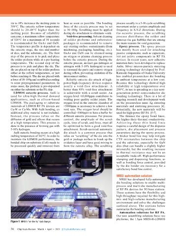
        Figure 1: MRSI’s “on-the-fly” tool changer.

        30   Chip Scale Review   March  •  April  •  2021   [ChipScaleReview.com]
        30

