Page 28 - ChipScale_Mar-Apr_2021-digital
P. 28
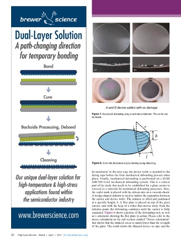
Figure 7: Successful debonding using a mechanical debonder. The carrier can
                                                            be reused.


                                                            Figure 8: Schematic illustration of glass bending during debonding.


                                                            be monitored. In the next step, the device wafer is attached to the
                                                            dicing tape before the final mechanical debonding process takes
                                                            place. Finally, mechanical debonding is performed on a SUSS
                                                            XBC300 Gen2 mechanical debonding system. This is a critical
                                                            part of the study that needs to be established for a glass carrier to
                                                            succeed as a material for mechanical debonding processes. Here,
                                                            the wafer stack is placed with the silicon side on a vacuum chuck.
                                                            A wedge-shaped initiator is used to initiate the separation between
                                                            the carrier and device wafer. The initiator is lifted and positioned
                                                            at a specific height, h. A flex plate is placed on top of the glass
                                                            carrier, and with the help of a roller that moves away from the
                                                            initiator point, the debonding continues until the carrier is fully
                                                            separated. Figure 6 shows a picture of the debonding tool, as well
                                                            as a schematic showing the flex plate in action. Please refer to the
                                                            stress calculation in the sub-section entitled “Stress calculation”
                                                            that shows that the induced stress is much lower than the strength
                                                            of the glass. The result shows the thinned device on tape and the

        26
        26   Chip Scale Review   March  •  April  •  2021   [ChipScaleReview.com]

