Page 29 - ChipScale_Mar-Apr_2021-digital
P. 29
debonded glass wafer that can be cleaned                              the pivot distance are listed in Table 2.
        to remove adhesive residues and recycled                              The smallest radius is 307mm when the
        multiple times, which is common practice                              lifting is 2mm and the pivot distance is
        for glass wafers used in laser debonding                              35mm. Figure 9 plots the relationship
        processes.                                                            between the radius of curvature and
          Edge t r i mm i ng and gr i ndi ng                                  the bending stress of glass wafer for
        conditions. Before bonding, an edge   Table 2: Calculated radius from typical lifting height   two thicknesses, 0.5mm and 0.7mm.
        trimming process was applied to the Si   and pivot distance values.   A horizontal, blue line indicates the
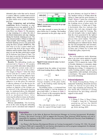
        wafer using a dicing saw tool (DFD6361)   to the edge strength to assess the risk of   typical, low-end edge strength value
        from Disco (see Figure 5). The purpose   glass failure due to bending. The bending   of glass wafers made by Corning. The
        of edge trimming is to reduce the risk of   stress generated on the glass edge can be   low-end strength value is much higher
        interfacial delamination and edge chipping                            than the stress generated by the tightest
        during the backside thinning process. The                             curvature 307mm during the debonding
        edge trimmed profile is 100µm in width and                            process (blue arrow marks). Therefore,
        50µm in depth. After bonding, a multi-step,                           the  glass  wafer  can  be  used  in  the
        backside thinning process was performed                               debonding process without failure. From
        using the Disco grinder (DGP8761). The                                the low-end strength line and curvature,
        first step is to use a coarse wheel grit                              the allowable bending curvatures are
        to remove the bulk of the excess wafer                                167mm and 234mm for 0.5mm and
        thickness until it reaches 92µm. The second                           0.7mm thick glass, respectively.
        step is to use the finer wheel grit to grind
        the Si thickness from 92µm to 52µm. The                               Summary
        final step is to use the finest grit to precisely                       For semiconductor wafer thinning,
        and slowly polish the Si thickness to the                             glass is an ideal carrier material because
        target thickness of 50µm.                                             of the following: 1) its ability to deliver
          Results. The debonding results are   Figure 9: Relation between the radius of curvature   variable CTE to match the wafer CTE;
        summarized in Figure 6. All samples   and the bending stress.         2) flexible thickness to minimize shape
        were successfully debonded, independent                               change during thinning and post-
        of the adhesive system used, and no   estimated from the radius of curvature   thinning processing; 3) transparency to
        damage was observed on the wafers.   with beam bending theory as Eq. 1 below:  enable bonding quality control; and 4)
        The images in Figure 7 show the intact                                compatibility with multiple debonding
        carrier and device wafers with some                                   technologies. This paper demonstrated
        imprints in the remaining adhesive layer                              successful debonding.
        at the initiator position, which is typical
        for mechanical debonding. The bulk   where  t is the wafer thickness,  E is   Acknowledgements
        adhesive is on the glass for material   Young’s modulus of the glass wafer,   We thank Hsiang-Hung Chang of
        A (device release) or on the device for   and r is the bending radius during the   Industrial Technology Research Institute
        material B (carrier release). Adhesive   debonding process.           (ITRI)  in Taiwan  for  providing Si
        residues or imprints of the initiator can   The bending radius, r, is obtained from   wafer edge trimming and thinning. We
        be removed in the subsequent cleaning   the lifting height, h, and the distance at   also thank MK Cornfield of Corning
        step. As mentioned above, the debonded   pivot from lifter, l, as shown in Table 2.   Incorporated for providing editorial
        glass carriers are in excellent condition   Eq. 2 is based on the assumption that the   support to this article.
        with no mechanical f laws. Af ter   deformation is simply cylindrical.
        removing the adhesive traces on the glass                             Reference
        surface, the carrier can be easily reused                               1.  J. Zhang, Y. Xiao, A. Teng, I. Dutta,
        with no issue.                                                            V. Singh, L. Yang, M. Li, “Advanced
          Stress calculation. The bending                                         packaging carriers for WLFO
        stress on the wafer during the debonding   The calculated radius of curvature   applications,” Chip Scale Review,
        process can be calculated and compared   r from the typical lifting height h and   pp. 20-26, Jul/Aug, 2019.


                       Biographies
                         Julia Brueckner is the Sales & Business Development Manager at Corning Incorporated, Wiesbaden,
                       Germany. She joined Corning in 2019 to support the Precision Glass Solutions (PGS) business unit and is
                       responsible for customers in the EMEA region. She received her PhD in Physical Chemistry from Heidelberg U.
                       Email  BrueckneJ@corning.com

                         Jay Zhang is the Business Development Director at Corning Incorporated in Corning, NY, USA. He joined
                       Corning in 2000 and is responsible for new business development as well as program management. He obtained
          his PhD in Applied Physics from Yale U. and an MBA from Cornell U.


                                                                                                             27
                                                             Chip Scale Review   March  •  April  •  2021   [ChipScaleReview.com]  27

