Page 25 - ChipScale_Mar-Apr_2021-digital
P. 25
sheet properties. If we assume the post-
        thinning wafer layer is significantly thinner
        than the carrier, the warp expression is:


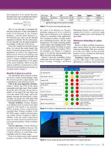
                                           Table 1: CTE values of commonly used wafer types.
          Here we use subscript s to designate the   the wafer to be thinned, its Young’s   Packaging Carriers (APC) product was
        material properties of the semiconductor   modulus engineered to be relatively   engineered to have a relatively high
        wafer to be thinned: E s  for Young’s   high, and its thickness to be optimized   Young’s modulus and a wafer thickness of
        modulus, t s  for the wafer thickness, υ s   within the constraints of the application.   up to 2mm.
        for Poisson’s ratio, and α s  for the thermal   The transparent nature of glass makes
        expansion coefficient. For the carrier glass,   laser debonding possible, and the same   Mechanical debonding of a glass
        we use subscript g for the same parameters   transparency also makes bonding quality
        accordingly. L is the size of the carrier.  control simple and straightforward. Other   carrier
          From the simplified formula shown   glass benefits include: the ability to reach a   Because of their excellent transparency,
        above, we can see the trends clearly. The   very low total thickness variation (TTV),   glass carrier wafers are often associated
        warp is linearly proportional to CTE   its reusability, etc. Figure 2  compares   with laser debonding. This does not have
        mismatch, as well as the temperature   glass to Si and the backgrinding tape   to be the case. Glass carriers provide
        differential between bonding and   (BGT) used for wafer thinning.     benefits for the mechanical debonding
        operation; it is inversely proportional to the   Figure 3  shows the availability of glass   process as listed below.
        carrier’s Young’s modulus; and the warp   wafers that cover the range of 3-13ppm°C   Enabling visual inspection. Glass
        is also inversely proportional to the square   from Corning. Corning’s Advanced   carriers add value to the mechanical
        of the carrier thickness. When we use the                             debonding by enabling visual inspection
        typical conditions encountered in wafer
        thinning and post-thinning processing, we
        see these trends in Figure 1.

        Benefits of glass as a carrier
          The discussions above focused on three
        levers for a carrier to help manage warp.
        We discuss specific requirements and
        constraints for each of the three below.
          CTE is the most important attribute.
        Table 1 shows the CTE of the most
        commonly used wafer types. These include
        Si on the low-CTE end, all the way to
        LiTaO 3  on the high-CTE end. Glass can
        cover the entire CTE range, and if the
        market warrants the investment, a glass
        company can design and make glass with
        very fine granularity, down to ~0.2ppm/°C.
          Young’s modulus. Young’s modulus
        is an effective lever to control warp when
        a perfect CTE match is not possible.
        While popular glass compositions   Figure 2: Comparison of substrates used for wafer thinning and their bonding properties.
        typically show Young’s modulus in the
        65-75GPa range, a highly technical glass
        can exhibit Young’s modulus as high as
        140GPa. In the real world, compromises
        must be made between performance
        and manufacturability, which translates
        into cost.
          Carrier thickness. Carrier thickness
        is another lever available to the user. The
        thickness-squared relationship makes
        it highly effective in controlling warp,
        especially in the 0.5-1.0mm range.
          Glass is an ideal carrier wafer material
        because it can offer a CTE that matches
                                           Figure 3: CTE and Young’s modulus of APC wafer products from Corning Incorporated.

                                                                                                             23
                                                             Chip Scale Review   March  •  April  •  2021   [ChipScaleReview.com]  23

