Page 19 - ChipScale_Mar-Apr_2021-digital
P. 19
package; and 2) for a heterogeneously-  with multiple RDL layers of an organic   the bridge dies and RDL layers. It
        integrated package that was to integrate   interposer have been developed to provide   can be customized for the various die
        the HBW memory with system on chip   the die to die interconnection feasibility   combinations with as many as 19 dies
        (SoC) dies within the same package.   and cost benefit without having to use   (with 9 bridge dies), and the basic 2.5D
        The 2.5D package was  introduced in   TSVs. Flexible and scalable designs that   structure with three dies (with one bridge
        early 2011 to immense interest on the   use more than three RDL layers for high   die), as illustrated in Figure 2c.
        part of many design houses. Amkor then   I/O density provide sufficient signal and
        announced its Silicon-less Integrated   power/ground line distribution [3,4]. But,
        Module (SLIM™) and its Silicon Wafer   as the chip module is getting larger, the
                                       ®
        Integrated Fan-Out Technology (SWIFT )   thermomechanical stresses generated
        package, which was a fan-out MCM—  between the die to die interfaces will
        but this technology had some limitations   break the RDL traces [10,12].
        and did not take off into production.   The fan-out technology called FOEB
        Then, TSMC introduced the integrated   provides localized high-density wiring
        fan-out (InFO) package for Apple’s A8   through the use of an embedded silicon
        processor, which was a fan-out package   bridge [13-19]. The partial bridge
        on package (FO-PoP). Subsequently,   interposer is applied in the specific area
        ASE also certified its 2.5D package for   of the high I/O density interconnection
        AMD at 2016. In 2017, SPIL overtook   that is used for the integration of HBM
        other outsourced semiconductor assembly   dies, which is in comparison to 2.5D
        and test suppliers (OSATS) as the first   packaging in which the whole piece of Si
        such supplier to manufacture 2.5D   interposer is used. Intel also demonstrated
        packages in high volume. In 2019, many   that the fan-out basis of EMIB technology
        semiconductor companies were offering   is capable of supporting high-bandwidth
        different versions of advanced packages,   interconnects with high-quality power
        which were actually the extension of 2.5D,   networks to the satisfaction of signal/
        FOMCM, and 3D packages. In 2020,   power integrity demand [20-22]. In signal
        SPIL introduced its FOEB that has been   integrity, both the insertion loss and near-
        certified in 2019 and started low-volume   end crosstalk show excellent agreement,
        manufacturing in 2020.             and the link power efficiency can be as
          2.5D  IC  with through-silicon via   low as 0.7pJ/b at 1.2V [22]. The solution
        (TSV) technology is the package that   not only offers high bandwidth, but also
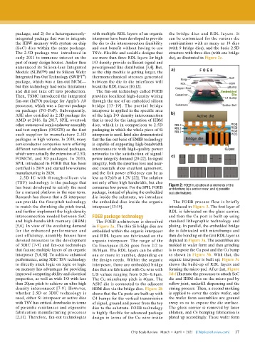
        has been developed to satisfy the need   consumes low power. For the SPIL FOEB   Figure 2: FOEB Illustration of a) elements of the
                                                                              architecture; b) a section view; and c) possible
        for a matured platform in the near term.   package, instead of placing the embedded   scalable features.
        Research has shown that a Si interposer   die inside the substrate, we introduce
        can provide the fine-pitch technology   the embedded dies inside the organic   The FOEB process flow is briefly
        to match the shrinking die pitch trend,   interposer [13-19].         introduced in Figure 3. The first layer of
        and further implement the high-density                                RDL is fabricated on the glass carrier,
        interconnection needed between SoC   FOEB package technology          and then the Cu post is built up using
        and high-bandwidth memory (HBM)      The FOEB architecture is described   standard lithographic technology and
        [5,6]. In view of the escalating demand   in Figure 2a. The thin Si bridge dies are   plating. In parallel, the embedded bridge
        for the enhanced performance and   embedded within the organic interposer   die is fabricated with microbumps and
        cost efficiency, assembly houses have   and RDL layers are fabricated on the   then die bonding on the first RDL layer as
        devoted resources to the development   organic interposer. The range of the   depicted in Figure 3a. The assemblies are
        of 3DIC [7-9] and fan-out technology   Cu line/space (L/S) goes from 2/2 to   molded in wafer form and then grinding
        that feature multiple layers of an organic   10/10μm. The RDL layers can be either   is to expose the Cu post and the Cu bump
        interposer [3,4,10]. To achieve enhanced   one or more in number, depending on   as shown in Figure 3b. With that, the
        performance, using 3DIC TSV technology   the design needs. Within the organic   organic interposer is built up; Figure 3c
        to directly stack logic on logic or logic   interposer, there are embedded bridge   shows the build-up of RDL layers and
        on memory has advantages for providing   dies that are fabricated with Cu wire with   forming the micro pad. After that, Figure
        improved computing ability and electrical   L/S values ranging from 0.56~0.8µm.   3d-f illustrate the processes to attach SoC
        properties, as well as wide I/O with less   The Cu microbump pitch is 40μm. The   die and HBM dies on the micro pad by
        than 20µm pitch to achieve an ultra-high   ASIC die is connected to the adjacent   reflow joint, underfill dispensing and the
        density interconnect [7-9]. However,   HBM dies via the bridge dies. Figure 2b   curing process. Then, a second molding
        whether 2.5D or 3DIC technology is   shows that the Cu posts are built up with   is applied to cover the entire wafer, and
        used, either Si interposer or active dies   C4 bumps for the vertical transmission   the wafer form assemblies are ground
        with TSV has critical drawbacks in terms   of signal, ground and power from the top   away so as to expose the die surface.
        of parasitic resistances and expensive   dies to the substrate. FOEB technology   The glass carrier is removed by laser
        fabrication manufacturing processes   is highly flexible for advanced package   ablation, and C4 bumping fabrication is
        [2,11]. Therefore, fan-out technologies   design in terms of the Cu wire inside   plated up accordingly. These wafer form


                                                                                                             17
                                                             Chip Scale Review   March  •  April  •  2021   [ChipScaleReview.com]  17

