
ficonTEC reveals an innovative 300 mm double-sided electro-optical wafer tester compatible with existing ATE and targeted at AI-driven silicon photonics
March, 2025 | ficonTEC Service GmbH, Achim Germany |An industry first, ficonTEC’s new 300 mm double-sided electro-optical wafer tester is compatible with existing semiconductor ATE architectures and is targeted at AI-driven silicon photonics computing demand.
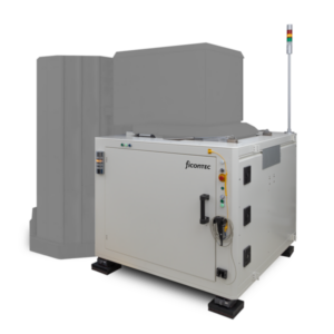
With immediate availability, this ground-breaking new technology enables high-throughput testing of silicon photonic integrated circuit (PIC) devices at wafer level. These devices are at the heart of the co-packaged optics (CPO) enabled photonic engines featured in the highest performance optical interconnects used within data centers. By implementing broad compatibility with existing ATE architectures, rapidly adoptable test capability is now commercially available for all major foundries facing the surging demand for contemporary and for recently announced next-generation CPO.
This new optical test cell directly docks with the ATE at a core software and hardware level, enabling DC and high-data-rate test capability on the top side and precision optical six-axis active alignment probing below. It also accommodates automatic wafer loading and incorporates a patented vacuum thermal control chuck assembly, in-situ fiber array calibration, end-face inspection, high-speed probe calibration, and automated PIC mapping.
Adoption is already in progress by a number of market leading chip manufacturers and foundries, noting that ficonTEC’s intention here is to maintain a broad and open compatibility with all leading ATE manufacturers. Further near-term activities will include developments for single-sided wafer formats as well as for die-level and module-level production test.
ficonTEC has established a global Sales & Service network that already serves around 1400 installed machine systems around the world – a good proportion of those systems have long contributed to the manufacture of high-end interconnect chiplets, and newer systems support the CPO-enabled formats currently utilized in 400G, 800G, 1.6T interconnects and beyond. ficonTEC is currently expanding its support network – in particular in Taiwan, Korea, Israel and USA – and boosting its presence globally to effectively address the rapidly accelerating take-up of new technology in the AI computing sector.
The new test cell and its variants form an integral part of ficonTEC’s evolving production capabilities specifically targeted at the CPO-enabled optical chiplet manufacturing workflow. 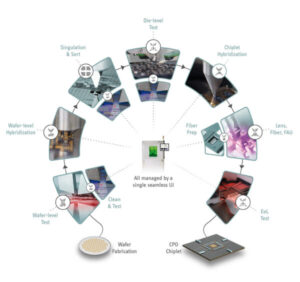 For the first time, a complete suite of highly cost-effective tools is now available for the entire CPO test and hybridization workflow, beginning with wafer-level PICs, continuing through die-level processes and ending with end-of-line packaging and module test. This production suite is essential in enabling new manufacturing benchmarks to be set for yield, time to market and ultimately TCO.
For additional information: info@ficontec.com