Page 8 - ChipScale_Jul-Aug_2020-Digital
P. 8
even laminate. The end result is a high-                              Xilinx FPGA noted earlier. Today, this
        performance pseudo-SoC built at a much                                technology is most commonly referred to
        lower cost in less time. A chiplet-based                              as 2.5D-IC packaging.
        design approach is very similar to what                                 About ten years ago, semiconductor
        we today call a package or SiP. But it’s                              foundries started to enter the world of
        also similar to designing a very small                                backend design, or what most now call
        printed circuit board (PCB) because each                              advanced packaging. The foundry-based
        chiplet will be built with a common/                                  approach of high-density RDL also drove
        known communication interface such as                                 renewed interest in fan-out wafer-level
        peripheral component interconnect (PCI),                              packaging (FOWLP), and now, with
        HBM, or advanced interface bus (AIB).                                 support for multiple die, interest is at an
                                           Table 1: Chiplet tradeoffs.        all-time high. Additionally, in an effort
        Where do we go from here?                                             to further increase bandwidth, 3D-IC
          So  far,  I’ve only  talked  about  the   heterogeneously integrated multi-chip   packaging – meaning wafer-on-wafer, or
        upside to a chiplet-based architecture.   products for decades. EDA companies   chip-on-wafer stacking – has new life.
        Now I’ll discuss some of the challenges.   started to develop tools for advanced   If we look at the chiplet trend more
        Even though designs are being built today   packaging in the early 1990s around the   closely, a key takeaway is that next-
        with multiple chiplets, the vast majority   time the ball grid array (BGA) provided a   generation chiplet-based technologies
        of this work is being done captively.   high-performance, small form factor option   are just a new way of partitioning logic
        That is to say, most chiplet-based   to the mechanical lead frame package.  that aligns nicely with advancements
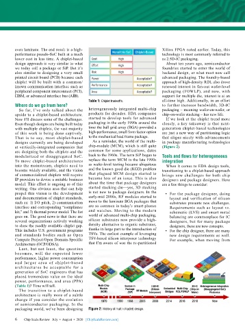
        designs currently are being developed   As a reminder, the world of the multi-  in package manufacturing technologies
        at vertically-integrated companies that   chip-module (MCM), which is still quite   (Figure 2).
        are designing both the chiplets and the   common for some applications, dates
        modularized or disaggregated SoC.   back to the 1960s. The term SiP began to   Tools and flows for heterogeneous
        To move chiplet-based architectures   replace the term MCM in the late 1990s   integration
        into the mainstream, chiplets need to   as wafer-level testing became ubiquitous   When it comes to EDA design tools,
        become widely available, and the vision   and the known good die (KGD) problem   transitioning to a chiplet-based approach
        of commercialized chiplets will require   that plagued MCM design started to   brings new challenges for both chip
        IP providers to devise a suitable business   become less of an issue. This is also   designers and package designers. Here
        model. This effort is ongoing as of this   about the time that package designers   are a few things to consider:
        writing. One obvious area that can help   started stacking die—yes, 3D stacking
        propel this vision is the development   is not new to package designers. In the   •  For the package designer, doing
        and documentation of chiplet standards,   early-mid 2000s, RF modules started to   layout and verification of silicon
        such as: 1) I/O pitch, 2) communication   move to the laminate BGA packages that   substrates presents new challenges.
        interface and corresponding “compliance   are so common in today’s smart phones   Requirements such as layout vs.
        kit,” and 3) thermal power model. The list   and watches. Moving to the modern   schematic (LVS) and smart metal
        goes on. The good news is that there are   world of advanced multi-chip packaging,   balancing are commonplace for IC
        several organizations actively working   silicon substrates now provide a high-  designers, but for many package
        to close the readily available chiplet gap.   density alternative to organic substrates,   designers, these are new concepts.
        This includes U.S. government programs   thanks in large part to the introduction of   •  For the chip designer, there are many
        and standards bodies such as Open   TSVs. The earliest example of leveraging   new design requirements as well.
        Compute Project/Open Domain-Specific   TSV-based silicon interposer technology   For example, when moving from
        Architecture (OCP/ODSA).           that I’m aware of was the re-partitioned
          Last, but not least, the question
        becomes, will the expected lower
        performance, higher power consumption
        and larger area of chiplet-based
        architectures be acceptable for a
        generation of SoC engineers that has
        placed tremendous value on the ideal
        power, performance, and area (PPA)
        (Table 1)? Time will tell.
          The transition to a chiplet-based
        architecture is really more of a subtle
        change if you consider the evolution
        of semiconductor packaging. In the
        packaging world, we’ve been designing   Figure 2: History of multi-chip(let) design.

        6 6  Chip Scale Review   July  •  August  •  2020   [ChipScaleReview.com]

