Page 12 - ChipScale_Jul-Aug_2020-Digital
P. 12
Electronic packaging for future electronic systems


        By Michael Töpper, Tanja Braun, Rolf Aschenbrenner  [Fraunhofer IZM]
        F        uture electronic systems like   approaches are artificial neural networks   theoretical computing power due to their


                 autonomous systems using
                 high-performance computing   and neuromorphic computing.     limited memory bandwidth. New hardware
                                                                              and software architectures are necessary
        (HPC) and edge computing systems,   Status of computing today         to break down the boundary between
        sensor-integrated systems and bio-   Today, a major part of computing is   pure logic and pure memory domains.
        integrated devices will require more and   performed in specialized data centers   This can be achieved by 3D stacking of
        more functions that cannot be managed   (cloud computing). Computing is executed   logic and memory on top of each other
        by  a single chip, even  if advanced   on highly parallel set-ups with thousands   and ultra-fast interconnections between
        system on chip (SoC) concepts are used.   of cores. Similarly, supercomputers are   the domains. Additionally, the technology
        Heterogeneous integration will be the next   built for large-scale calculations mainly in   of embedding integrated circuits (ICs)
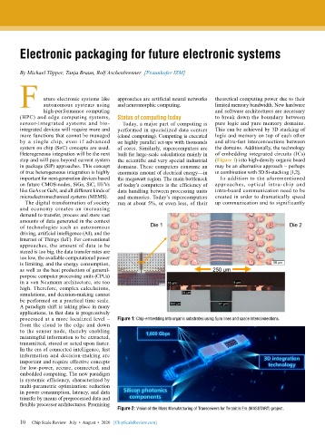
        step and will pass beyond current system   the scientific and very special industrial   (Figure 1) into high-density organic board
        in package (SiP) approaches. This concept   domains. These computers consume an   may be an alternative approach – perhaps
        of true heterogeneous integration is highly   enormous amount of electrical energy—in   in combination with 3D Si-stacking [1,2].
        important for next-generation devices based   the megawatt region. The main bottleneck   In addition to the aforementioned
        on future CMOS-nodes, SiGe, SiC, III/Vs   of today’s computers is the efficiency of   approaches, optical  intra-chip  and
        like GaAs or GaN, and all different kinds of   data handling between processing units   intra-board communication need to be
        microelectromechanical systems (MEMS).  and memories. Today’s supercomputers   created in order to dramatically speed
          The digital transformation of society   run at about 5%, or even less, of their   up communication and to significantly
        and economy creates an increasing
        demand to transfer, process and store vast
        amounts of data generated in the context
        of technologies such as autonomous
        driving, artificial intelligence (AI), and the
        Internet of Things (IoT). For conventional
        approaches, the amount of data to be
        stored is too big, the data transfer rates are
        too low, the available computational power
        is limiting, and the energy consumption,
        as well as the heat production of general-
        purpose computer processing units (CPUs)
        in a von Neumann architecture, are too
        high. Therefore, complex calculations,
        simulations, and decision-making cannot
        be performed on a practical time scale.
        A paradigm shift is taking place in many
        applications, in that data is progressively
        processed at a more localized level –   Figure 1: Chip-embedding into organic substrates using 5µm lines and space interconnections.
        from the cloud to the edge and down
        to the sensor node, thereby enabling
        meaningful information to be extracted,
        transmitted, stored or acted upon faster.
        In the era of connected intelligence, fast
        information and decision-making are
        important and require effective concepts
        for low-power, secure, connected, and
        embedded computing. The new paradigm
        is systemic efficiency, characterized by
        multi-parametric optimization: reduction
        in power consumption, latency, and data
        transfer by means of preprocessed data and
        flexible processor architectures. Promising
                                           Figure 2: Vision of the Mass Manufacturing of Transceivers for Terabit/s Era (MASSTART) project.

        10
        10   Chip Scale Review   July  •  August  •  2020   [ChipScaleReview.com]

