Page 16 - ChipScale_Jul-Aug_2020-Digital
P. 16
allow an upscaling of the system size to
        a large number of wafers with reasonable
        effort, a full-wafer embedding concept
        for printed circuit boards was developed.
        The wafers were thinned to 250µm and
        laminated with additional prepreg layers
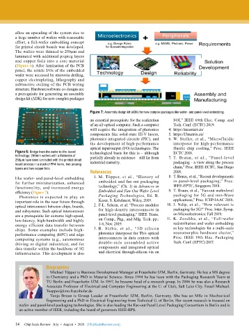
        and copper foils into a core material
        (Figure 6). After lamination of the PCB
        panel, the reticle I/Os of the embedded
        wafer were accessed by microvia drilling,
        copper electroplating, lithography and
        subtractive etching of the PCB wiring
        structure. Hardware/software co-designs are
        a prerequisite for generating an assembly
        design kit (ADK) for new complex packages


                                           Figure 7: Assembly design kit (ADK) for new complex packages like wafer- and panel-level embedding.
                                           an essential prerequisite for the realization   SOI,” IEEE 69th Elec. Comp. and
                                           of an all-optical computer. Such a computer   Tech. Conf. (ECTC) 2019.
                                           will require the integration of photonics   4. https://masstart.eu/
                                           components like solid-state III-V lasers,   5. https://l3matrix.eu/
                                           photonics integrated circuits (PIC), and   6. W. Steller, et al., “Microfluidic
                                           the development of high-performance    interposer for high-performance
                                           optical input/output (I/O) technologies. The   fluidic chip cooling,” Proc. IEEE
        Figure 6: Bridge from the wafer-to-the-board   technological basis for this is – although   ECTC 2018.
        technology: 200mm wafers with a thickness of   partially already in existence – still far from   7. T.  Braun,  et  al.,  “Panel-level
        250µm have been laminated with the printed circuit   industrial maturity.  packaging - a view along the process
        board process in a stack of FR4 frame, two prepreg
        layers and two copper foils.                                              chain,” Proc. IEEE-ECTC, San Diego
                                           References                             2018.
        like wafer- and panel-level embedding   1. M. Töpper, et al., “History of  8. T. Braun, et al., “Recent developments
        for further miniaturization, enhanced   embedded and fan-out packaging    in panel-level packaging,” Proc.
        functionality, and increased energy    technology,” (Ch. 1) in Advances in  IEEE-EPTC, Singapore 2018.
        efficiency (Figure 7).                 Embedded and Fan-Out Wafer Level  9. T. Braun, et al., “Fan-out wafer-level
          Photonics  is  expected  to  play  an   Packaging Technologies, Ed. B.  packaging for 5G and mm-Wave
        important role in the near future through   Keser, S. Kröehnert, Wiley, 2019.  applications,” Proc. ICEP-IAAC 2018.
        optical interconnect between chips, boards,   2. F-L. Schein, et al. “Process modules  10. I. Ndip, et al., “How relevant is
        and subsystems. Such optical interconnects   for high-density interconnects in  packaging for 5G?” Proc. Inter. Symp.
        are a prerequisite for extreme high-speed,   panel-level packaging,” IEEE Trans.  on Microelectronics: Fall 2019.
        low-latency, high-bandwidth and highly   on Comp., Pkg., and Mfg. Tech. pp.:  11. K. Zoschke, et al., “Full-wafer
        energy efficient data transfer between   1-6, Nov. 2019.                  redistribution and wafer embedding
        chips. Some examples include high-   3. B. Si rbu, et al., “3D silicon    as key technologies for a multi-scale
        performance computing (HPC) and edge   photonics interposer for Tb/s optical  neuromorphic hardware cluster,”
        computing systems (e.g., autonomous    interconnects in data centers with  Proc. IEEE 19th Elec. Packaging
        driving or digital industries), and for   double-side  assembled  active  Tech. Conf. (EPTC) 2017.
        data transfer within the backbone of 5G   components and integrated optical
        infrastructures. This development is also   and electrical through-silicon via on


                       Biographies
                         Michael Töpper is Business Development Manager at Fraunhofer IZM, Berlin, Germany. He has a MS degree
                       in Chemistry and a PhD in Material Science. Since 1994 he has been with the Packaging Research Team at
                       TU Berlin and Fraunhofer IZM. In 1997, he became head of a research group. In 2006 he was also a Research
                       Associate Professor of Electrical and Computer Engineering at the U. of Utah, Salt Lake City. Email Michael.
                       Toepper@izm.fraunhofer.de
                         Tanja Braun is Group Leader at Fraunhofer IZM, Berlin, Germany. She has an MSc in Mechanical
                       Engineering and a PhD in Electrical Engineering from Technical U. of Berlin. Her recent research is focused on
          wafer- and panel-level packaging technologies. She is also leading the Fan-out Panel Level Packaging Consortium in Berlin and is
          an active member of IEEE, including the board of governors IEEE-EPS.


        14
        14   Chip Scale Review   July  •  August  •  2020   [ChipScaleReview.com]

